Continue to Site

Welcome to EDAboard.com

Welcome to our site! EDAboard.com is an international Electronics Discussion Forum focused on EDA software, circuits, schematics, books, theory, papers, asic, pld, 8051, DSP, Network, RF, Analog Design, PCB, Service Manuals... and a whole lot more! To participate you need to register. Registration is free. Click here to register now.

DC-DC Converter needed

Status
Not open for further replies.

Lavanya R

Junior Member level 2
Joined
Dec 15, 2014
Messages
22
Helped
0
Reputation
0
Reaction score
0
Trophy points
1
Activity points
161
Hello Friends,

I am new here... I want to design buck converter where can be adjustable DC output voltage using buck converter that regulate voltage using switching element (preferably MOSFET) driven by PWM technique using timer 555 converter. PWM technique is applied to switch the transistor fully on and fully off.

The specifications are:

Input voltage: 60V (min) DC
Input current: 10 A
Output current: 10 A
Output voltage: varies as per the duty cycle.
Duty cycle range: 10% to 100%


Please help me out with circuit diagram and component values.
Thanks in advance:grin:
 

It is possible to voltage-control a 555 duty cycle. Is this the part of the project you need help with?

The higher the voltage at the control pin, the longer the duty cycle.

As for the buck converter, see the thread below. Look for my posts containing links to tutorial circuits. These are animated and interactive. A buck converter is one of them.

https://www.edaboard.com/threads/268178/
 

DC-DC converter schmatics

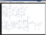
View attachment 11.pdf

Pls verify the attached schematics and request for corrections so it works asper my requirement

thanks in advance:lol::lol:
 

Hi,

I went through your pdf. i suppose this is like a some what an open loop design as i see no feedback path to regulate the output voltage to guard against variations that may arise due to load fluctuations.

That means as the load varies you may have to manually vary the duty cycle to cope up with regulation.


The design requirement is some what not clear to me,

Vin min and Vin max to specified.

Seems output voltage not fixed, better fix to some value. So duty will be D=Vout/Vin approx

& fix switching frequency in 555 timer design to your choice say in range of 100kHz to 500kHz may be

the output current is specified like 10A, which even if Vout=3.3V amount to 33W output power, need to be pretty careful selection and layout of MOSFET.

The MOSFET driver NCP IC is synchronous drive , so do u really need the diode as well as bottom MOSFET together?

Inductor rating may be a quick estimation can be done using,

V=L*di/dt

L=[(Vin-Vout)*dt]/di

Inductor ripple current can be fixed as di=40% of output current , 10*0.4=4A, dt is ON time calculate from frequency and duty cycle

Average inductor current =output current=10A, ripple current =4A So some what i would put current rating of minimum 12A rated inductor.


This are my quick estimations ..may be useful.. but i strongly suggest you go through the design procedure of a standard buck converter..
 

Many PWMs have a min, max or both-ends duty cycle limit.
A sawtooth timing ramp requires at least one end to "bury"
the return ramp interval. Blanking features will either make
a min on time, or make the transition from 0% to N% "notchy"
as you cross the blanking edge.

You can design a 0 - 100% PWM simply but simple is not the
norm in power management ICs anymore.

You have to ask yourself some questions, such as how
important it is that the output be smoothly variable from
0.0 to ?.?V, or whether you could have some low voltage out
region where you'd forgive things like instability and nonlinear
control:eek:ut transfer function. Depending on what you decide
your solution could be simple, or not so much.
 

Hi,

Thanks for your suggestion. could you help me with feedback circuit diagram so that manual voltage regulation can be avoided.

thanks in advance.::smile:

- - - Updated - - -

Also maximum Input voltage is 100 V
 

Hi,

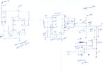
As per your suggestion I modified my circuit diagram. but not sure about feedback section which can provide closed loop operation. I am attaching the modified circuit diagram.

Help me out for the feedback circuit. ckt1.jpg

Thanks in advance:-D
 

Input voltage: 60V (min) DC
Input current: 10 A
Output current: 10 A
Output voltage: varies as per the duty cycle.
Duty cycle range: 10% to 100%

it sounds like you have a pwm "signal", which you want to use to vary the output voltage?

I would filter the signal to produce DC. tHEN I WOUld USE THAT DC SIGNAL AS AN INPUT TO AN external ERROR AMPLIFIER which was regulating the output voltage.......and the external error amplifier output would be fed into a pwm controller which would vary the switching duty cycle of the power fet in order to give the requisite output voltage.

I don't think you need a 555 timer, unless you are using the 555 timer to give the pwm signal?......I assume you don't want to drive the power fet directly with the 555 timer?
 

The circuit in post #8 doesn't work with IR2110:
- inversion of HIN or LIN signal required
- no deadtime generation

To implement variable PWM based on voltage feedback, a standard PWM controller like SG3524 would be the best solution.
 

It appears that you aimed at a 3.3V DC output according to the feedback values. The inductor seems way to big and the capacitor too small to get a well behaved output.

The feedback and compensation values you show will make the control slow with lots of overshoot on dynamic load changes.
Attachment FB_1 shows this response. (the square wave shows the dynamic load switch control from 5A to 10A)

The next attachment FB_2 is with a 40uH inductor and a 1000uF capacitor. You can see a good phase margin and better response with different compensation values. The capacitor will most probably need to be increased a lot more to meet specifications for a safe 3.3V supply.
 

Attachments

  • FB_1.png
    FB_1.png
    41.4 KB · Views: 83
  • FB_2.png
    FB_2.png
    39.7 KB · Views: 79

Hi all,

Thanks for your suggestions.
Based on the inputs, I modified my circuit. the same is been attached.
But now I am facing a problem that when I turn on my circuit, the output across capacitor increases, measured using DMM and stops to a value of 12V. But the same circuit works just fine if it is simulated in Proteus demonstration. Kindly check the circuit and help me out.

Thanks in advance11.jpg
 

I fear, it's simply unrealistic to expect stable low voltage output without voltage feedback.
 

but during proteus simulation the circuit works properly such that voltage varies from 0V to 30V as per the change in pot's wiper without feedback circuit. but practically it is not happening
 

This happens because your simulation is ignoring important parameters of a real circuit like parastic inductances and capcitances.
 

so how can I resolve this issue.. are the components values which I have selected are correct??
 

The 555 used as inverter has about 200 ns propagation delay according to datasheet and causes overlapping HIN and LIN pulses. MOSFET specification is unknown, but the asymmetrical gate circuit is most likely not sufficient to compensate the negative deadtime. Shootthrough may be one reason for getting unexpected circuit behaviour.

But apart from this problem, design must be aware of non-ideal cicruit parameters. The usual conclusion is to implement feedback and not to rely on an ideal duty cycle to output voltage characteristic.
 

Status
Not open for further replies.

Similar threads

Part and Inventory Search

Welcome to EDABoard.com

Sponsor

Back
Top