Continue to Site

Welcome to EDAboard.com

Welcome to our site! EDAboard.com is an international Electronics Discussion Forum focused on EDA software, circuits, schematics, books, theory, papers, asic, pld, 8051, DSP, Network, RF, Analog Design, PCB, Service Manuals... and a whole lot more! To participate you need to register. Registration is free. Click here to register now.

DC-DC converter isolation, questions from a newbie.

Status
Not open for further replies.
Okey I will be very determined to follow the step-by-step approach so I will now only concern my self with controller features I want, and order all other needed parts for the primary. Maybe I need to write a "must have" list for finding a controller.
Now I am just throwing stuff out there.

1, synchronization to other controller possible.
2, current mode control.
3, cycle-to-cycle current limiting.
4, adjustable duty cycle.
5, adjustable dead-time.
.
1/Any of the controllers can be synchronized, methods vary, but if you read the application notes they tell you exactly how to do it.
2/ Current mode control offers many advantages and is definitely recommended for something like this.
3/ Current mode gives you very fast cycle by cycle limiting for free.
4/ Current mode gives you voltage adjustable duty cycle.
5/ With single ended flyback, no dead time is required.

There are dozens of controllers out there that would work fine. The one I usually use is the 3825.
It has optionally current mode or voltage mode control, and the two outputs can be connected to give either an 0-50% or 0-100% maximum duty cycle.

Its difficult to plan far into the future right to the end with a project like this.
Best to start off with something very basic, test it, learn from it and experiment.
Then gradually develop a few ideas, and it will all take on a life of its own.
 
  • Like
Reactions: David_

    David_

    Points: 2
    Helpful Answer Positive Rating
Yes I just had a thought along those lines, ferrite cores used for my targeted application and power levels cost to much to buy a single core without qualified knowledge that it is what I need. But what if I design a circuit that operate over the voltage range I want only at low currents so as to dramatically decrease the output power?

That should allow me to by a couple of different cores to experiment with to learn from, could that be a good idea?
I have to little knowledge to determine if the high power levels that in the end will be used will change things or if my time with low power cores will provide valid results and insights?
 

Easy enough to start out with whatever core you can lay your hands on.
Something out of a big old TV maybe ?

Work out how many turns that core needs to have on the primary, and select a wire size that uses about half the available winding area, or maybe just a bit less.

You then just gap that core to give the required inductance.
How much power it can safely run is determined only by the allowable temperature rise.
 
  • Like
Reactions: David_

    David_

    Points: 2
    Helpful Answer Positive Rating
I am have for more than a year now tried to learn about ferrite and cored inductors but without any great success but I start to feel as if I manage to go through a design iteration of a core I can actually start to understand what I have been reading about for so long. And in that way I'd like to not use any unknown cores available to me even though I have maybe 40 ferrite transformers scavenged from computer supplies and such and instead by some small core to have the specifications to do it properly, even though I could do some measurements to find out what I need. We shall see what I can find and if its cheap enough I'll just by two kinds of core or something.

And for the application I had in mind, this is a circuit that I have made a prototype of and am in a rather outdrawn process of developing a program for using a Arduino Due, though I will try to implement the real deal with a ATxmega later on.
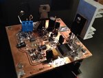
I have done some quite large rework on the prototype but this schematics reflects the working circuit, Klaus if you are reading this I'd like to ask you if you know what could cause my circuit to have a minimum output voltage of 5,5V?
Previusly I hade used your solution successfully but when I this time did it again to tailor it to the 32V input suddenly when the DAC is at 0V(inverted) the output is 5,5V. So far I don't know why.
linear.png 1.jpg 2.jpg
 

I have on more than one occasion gotten access to this falstad.com simulator which appears a great tool for learning however I continually struggle with enabling Java on my browser but I can't get it running.

I understand. My PowerMac (running OS 10.5.8) has become outdated, and lately I'm getting problems running Falstad's simulator at his site.

Don't know what you need to do to your computer so that Java can run.

Does it get simpler if one goes from designing for 0-60V to 10-60V(10-55V actually)?

I made my power supply 0-16V continuously variable. 3A max. Linear drop.

It has worked out ideal, for the most part.

To me it is vital that it goes all the way down to 0V.

And the range, up to 16V, is ideal for the components I usually work with. I don't destroy IC's accidentally as I turn the knob. Etc.
 

Warpspeed, I would like to ask you to take a look at a PDF and answer a question about one parameter. Anyone are of cource welcome to do so and I would really appreciate a clarification here.
It is a datasheet for a ferrite E core:
http://www1.elfa.se/data1/wwwroot/assets/datasheets/B66329-G-X187_eng_tds.pdf

At the first page in the first table(Ungapped), in the fifth column they specifies something as .
There are two rows one for material N27 and one for N87, oh well here is a description of it that was really painful to make, so painful I wonder why I did it and feel like slapping my self for wasting so much time.

Ungapped
----------------------------------------------------------------------------------------------
Mate| Al value nH ----- | -µe -| Al1min(nH)| ----------- Pv W/set ------------- |
----------------------------------------------------------------------------------------------
N27 | 4750 + 30/–20 % | 1560 | --- 3800 ---- | < 4,40 (200 mT, 25 kHz, 100°C) - |
----------------------------------------------------------------------------------------------
N87 | 5200 + 30/–20 % | 1690 | --- 3800 ---- | < 12,00 (200 mT, 100 kHz, 100°C)|
----------------------------------------------------------------------------------------------

I don't know what I should make of this and how to deduce which of the materials is more suitable for me(other than the quoted of 25kHz), about that Pv W/set, does it say something like the core being able to handle below 4,4W with a flux density of 200mT at 25kHz during a temperature of 100°C?
I read and I read and I read but this subject is of inductor cores are so wide and contains so many different things that I have never had this much trouble with any other subject. It is as if the subject is so wide and the things to keep in mind to get it all to fall in place builds and builds until my limited concentration is like a bubble getting bigger and bigger while thinner and thinner and never do I reach any understanding before the bobble pops.
That is actually how I experience ADD, if I get to many things to keep in mind it just falls apart into nothing.

Anyway any clarification would be a enormous help for me.

Regards
 

David, its a real Jungle, and all very confusing I agree.

First thing, the N27 material is pretty old, its a typical "power ferrite" similar stuff to what perhaps a dozen other ferrite manufacturers have been making for a very long time.

In more recent times, particularly with the invention of mosfets, switching frequencies are pushing higher and higher, and the ferrite manufacturers have responded with improved materials that have far lower loss at 100 Khz and well above that.

If you are planning to build something to run below 30Khz, either material will work very well, and there will be no detectable difference between choosing either the N27 or N87 material.

There is a very slight difference in the permeability and the Al value (inductance per turn) ungapped, but as soon as you gap it, that difference also disappears.

So either material is suitable at the low frequency end, just buy whatever you can, and it will work fine.

At 20 Khz any ferrite material will be saturation limited, you need not worry about core heating or losses. Just put on enough turns to get you in the 200mT flux range and you will be in business.

At 100C the core will saturate at a lower flux level than at 20C.
What they are telling you is that the N27 material will still work at the full rated 200mT and 100C at 25Khz.
But at higher frequency or higher temperature than that, that 200mT will need to be de-rated.

The N87 material hits the same brick wall, but at the much higher frequency of 100 Khz.
 
Last edited:
  • Like
Reactions: David_

    David_

    Points: 2
    Helpful Answer Positive Rating
I see, its a good thing that this jungle happens to be very interesting so one has a incentive to not give up.
I will buy a small core and implement a prototype but I have one thought, while reading different documents it is kind of made clear that different rules in core choice apply to different topology's. Since I am going for a diagonal half bridge flyback design is the notes for single switch flybacks relevant for me?

Or do my design have anything to do with the half bridge topology?

The time when the primary are effectively removed from the circuit through opening the switches is refereed to the flyback time(or flyback something), period maybe. While still reading about flybacks I see references to a forward(time, period or whatever), the flyback part is is referring to the flyback action which flips the polarities and dumps the energy into the secondary inductor, but what is the "forward" part about?

I have begun to feel optimistic about the transformer design which before was a nightmare, I will make this work and I want to thank you for your guidance which has been vital so far and extremely valuable for me in order to see through this jungle.
Thanks

- - - Updated - - -

Here I found a great tool to explore cores and materials:
http://en.tdk.eu/tdk-en/180490/design-support/design-tools/ferrites/ferrite-magnetic-design-tool
I have been playing with it for a little while but not explored more than a little part but it seems most useful.
 

Since I am going for a diagonal half bridge flyback design is the notes for single switch flybacks relevant for me?.
Yes fully relevant.

The only difference is that the half bridge diagonal topology is fully protected from overvoltage by clamping the switching devices to the incoming dc supply rail.

The single ended flyback topolgy can self destruct when the swtiching device turns off if there is nowhere for all the stored energy in the inductor to go.
The back EMF voltage spike this produces can rise to destructive levels.
This can very easily happen with a bench power supply if your load suddenly drops off at full flat out power.

So its a much safer and foregiving design to work with for this type of bench power supply application.

There are different transformer design rules for different topolgies.

For instance, a push pull forward converter drives the core in both directions.
A single ended forward converter only drives the core in one direction, so you have to allow in your design for only half the flux swing. Maybe 400mT for push pull, 200 mT for single ended.

Flyback converters will need an air gap to reduce the inductance. You must always fit enough turns on to not exceed the required flux swing, usually 200 mT.

But doing that, always produces a lot more inductance than is wanted.
So you get to reduce the inductance by fitting an air gap without changing the number of turns, which cannot be done

While still reading about flybacks I see references to a forward(time, period or whatever), the flyback part is is referring to the flyback action which flips the polarities and dumps the energy into the secondary inductor, but what is the "forward" part about?
The forward part ramps up the stored magnetic energy in the core, with a rising current ramp in the primary.
When your switching device turns off, the collapsing flux then generates a falling current ramp in the secondary.

Energy is not coupled directly from primary to secondary as it is in a normal transformer. In a flyback, its a two stage process separated in time.
An energy storage phase, and then an energy release phase.
It then just cycles back and forth, storing and releasing the stored energy.
 
  • Like
Reactions: David_

    David_

    Points: 2
    Helpful Answer Positive Rating
Thanks for the clarification.

I think I have a rather large problem, using the IR2110 will not work as far as I know, its uses a capacitor to increase the voltage for turning on the high side switch BUT the charging of this cap is depending on the high switch being in its OFF state while the low switch is in its ON state to pull the high side "0V" reference pin to GND. That's the VS pin.
And since I need both switches to work in there ON state at the same time... Its not going to work.

I really want to avoid having to deal with another transformer to power the switches, do anyone know of a solution for this dilemma?

Regards
 

The IR2110 will work fine in your diagonal flyback circuit, I have done it that way myself many times.
As you know, both mosfets are supposed to turn on simultaneously.

If the upper mosfet initially has no gate drive power, which is almost a certainty, then just the lower one turns on normally by itself, the top one remaining "off".

This grounds the source of the upper mosfet through the primary (for that very first start up cycle only). That charges up the top gate drive supply through the diode.

The first "on" cycle will be a dud, but it does get power supplied to the upper mosfet gate driver.
The second "on" cycle will be normal with both mosfets turning on together, and with full forward voltage across the primary, and you are away !

In fact normal half bridge circuits operate the same way. The top mosfet can get no gate drive power until the lower mosfet turns on for the first time.

The only difference is that you have the primary between the upper and lower mosfets, a normal half bridge has a direct connection.
But otherwise getting gate drive power to the upper mosfet at initial startup is pretty much the same for both circuits.
 
  • Like
Reactions: David_

    David_

    Points: 2
    Helpful Answer Positive Rating
That's just great, thanks.
I am in the process of making a order for parts for my first version/prototype and I just wonder if I can do this prototype DIY style without a real PCB cous I have read that you should not do that since SMPS is such a sensitive system for noise and such so the prototype then is not reliable. I was thinking about if I should choose DIP or SOIC but then I remembered "I can etch my own PCB" which has worked in the past. I really like SMD, everything gets so much more neat with them most of the time.
Though I get in trouble when I need to etch footprints like VSSOP or µMAX but this time I will see to it that my board have more free space in the etching "tub".

But the question is still valid because I don't know how layout-sensitive a design at 25kHz is(I think there was something that makes me do it 25kHz and not 20kHz but that would hardly matter would it.)

But the diagonal bridge type of flyback would mean thst I can get away with 400V MOSFETs then?
I feel that is kind of cutting it to close perhaps, who knows what spikes might occure and from where but buying for the prototype I can get 10 400V 4A N-channel MOSFETs for the price of 1 other 400V, 500V or 600V MOSFET so if I can manage with them for now that would make it much cheaper.


Regards
 

The way I build my prototypes, I bolt the mosfets onto a fairly large flat sheet of aluminium, along with the diodes, transformer, input filter capacitor and all the other high voltage, high power stuff. All with very short direct wiring.

I then carry the gate and source connections away through a twisted pair which can be reasonably long, to the "control system" which initially might be one of those white bread boards where you poke the components into holes.

When satisfied with that, version #2 might be soldered together on a piece of matrix board, which is a bit more robust, and less likely to have components either fall off or short together.

When its all finally working, and you know EXACTLY what is needed, a circuit board will add further reliability, and essentially the project is then complete.

Surface mount is definitely better for mass production, but for a one off home project, its a lot more trouble than it is worth IMHO.
Normal sized radial leaded components, and DIP ICs (all in sockets) are a lot more practical.
IC sockets allow reuse of the same ICs in future projects, from scrapped prototypes, as well as easy fault diagnosis and repair if the smoke does escape...

The big advantage of the diagonal topology is that the mosfets are pretty well protected from overvoltage.
When (not if) you start blowing up mosfets, it will almost always be from overcurrent. So just use real cheapies, and get plenty of them.

A bit further into the project when you start to get serious and push a bit more power, and you are through the blowing up lots of mosfets stage, something a bit bigger may be worth investigating.
 
Last edited:
  • Like
Reactions: David_

    David_

    Points: 2
    Helpful Answer Positive Rating
I don't know if one does it like this or if I should start a new thread about the topic of the transformer but if I continue the topic here this could become more useful to anyone in my previous position as it goes from the start(kind of).

I am about to check out an order for a couple of ETD43 cores made out of N27 and three bobbins, together with cheap 0,1% resistors sold on sale, I'm sure its not a special price if one would buy thousands but <100 price its nice. Its from Elfa distrelect if anyone one is interested.

Anyway the only thing keeping me from checking the order out is Enameled copper wire, which to buy?

I ask because I am wondering if maybe it is a good idea to oversize the copper width to gain better heat dissipation or if there are any other consideration that I should be aware of when selecting wire for the transformer. Its good I am going for low frequency since at the time litz it out of my budget range, a guide from a core manufacturer indicates that this core is good for 151? They call it Ptrans and it has to do with the power handling capability of the core but they do nowhere say Whats or any other quantity but I assume its 151W which would make it good for delivering at least 50W in a flyback right?

I have gotten the idea that cores are specified for W in some way where you need to adjust that value depending on topology and for flyback you have to de-rate that W to 0,3, lets say 0,33 to take a third = 50W.

By the way, Warpspeed mentioned the 3825 controller and I have been wondering why there are two outputs and there are 3825 and then 3823 which is specified as 0-100%Duty ratio opposed to 0-50%.

Also different in different controllers are the phase or polarity of the outputs, ether they are the same or they are in opposite polarity(in this regard I think you might as well look at it as having a large phase shift...)
The datasheet surly does not mention how one would use the two output to get ether 0-50% or 0-100% D, I feel as these controllers are capable to many things never mentioned in the datasheet/datasheets. Do you have any literature that explores these/this controller?
Or is the only way to in depth get into the controller and for your self figure out how to take advantage of things and simply by knowledge about electronics know what I can do?

I appreciate the description of prototyping, if you at some time would be able to I would love to see a picture of that large flat sheet of aluminium because I have a hard time envisioning how it is actually done.

But for my prototype for the circuit in this thread I think I will try to etch a simple flexible PCB(flexible means I will make room for multiple choices for components and make it very changeable through jumpers/extra footprints) I know that from a outside perspective this can seem as a strange and not at all good way to do this kind of thing but my ADD+ aspberger makes such prototyping hard. I use to do this kind of prototyping:
bildprotocoil.JPG

Or similar only on a un-etched(cleaned from fotoresist) PCB which I work on with scalpel and a "multi-tool", you know one of those high RPM machines with plenty of different tools to be mounted on it, from brushes to cutting disks and polishing tools.
But for one thing I learn more easily if going the etching way and I have still no control over the autism in my person and I can sit down to solder something and then snap out of it 8hours later without having eaten, no water no nothing and I spend hours and hours on ridiculous details that does not matter and is not even relevant for the circuit. But it is not in my power to say "Now I'll stop" even if I feel physicly sick I go on for hours, strange as h**l but apparently a classic autism trait.
Motivated by that I am trying to find a way of doing good prototypes with home-etching tools without having to make 10 versions, we shall see if I can manage that or not.
 

What sized wire to use in your transformer ?
There are several things to bear in mind.

The first is that there is only so much room on the bobbin, and when you have worked out the minimum required number of turns, the wire size that will fit in the available space limits the maximum wire size.
The wire needs to be a certain minimum size to carry the rms current, otherwise it will overheat. About 5 amps rms per millimetre squared is about the limit.
Skin effect causes current to flow mostly only near the surface of the wire. If you need a lot of current at high frequency, multiple thin wires is the way to go. At your power level single wire primary is all that is needed.

The ultimate power rating of a transformer depends on temperature rise, which depends on how much copper you can fit into the available space.
If you need several different windings, with insulation between, that limits the amount of copper, and reduces the power rating.
Its all about the most efficient use of space.

There are many different controllers, and all have certain features that make them particularly attractive for certain topologies and applications.
But if you are experimenting at home, its best to stick to the more common types and base your designs on something you already may have have several of.
The two output types are probably more useful, because they can either be used as 0-50% dual output, or both outputs combined to provide 0-100 % single output. Its easy enough to invert the outputs by using an inverting gate driver chip.

You will often find that the more common types often cost less and are much more readily available, so its probably best to stick to those for a home project. If you need to add a few extra parts to make it do exactly what you want, that is not such a big problem.
 
  • Like
Reactions: David_

    David_

    Points: 2
    Helpful Answer Positive Rating
So I have trouble making up my mind about something.
The order for the core and FETs and such is being delayed but in the mean time I have been looking through the datasheets about the 3825 ICs and they all show a circuit said to be "This test fixture is useful for exercising many of the
3825’s functions and measuring their specifications."

Any way what I am unsure of if this: First I will run the circuit with battery's or some other power source to see if all is good BUT then, is it worth anything doing tests on the circuit with a separate stable power source or should I proceed to powering a circuit from the mains and the transformer using only a primary and a auxiliary to power the PWM controller(with plexiglass between me and the circuit:) ) or only the primary and still supply the "aux-supply" from a separate stable power source ei a battery or such?

It is somewhat unnerving with mains circuit although I do know enough to be safe, but I guess that's a good thing that keeps you from making stupid and dangerous mistakes.

Regards
 

For me at least, its always a multi step process working up a new design from scratch.

First stage is to build just the control section and power that off a 12v bench power supply. I can then check the operating frequency, look at the gate drive waveforms, and test any current limit circuits, soft start, and any other features.
Duty cycle control to be adjusted manually by a potentiometer at the early stage.

Next attach it to the power section, mosfet, heat sink, transformer, output rectifier. Power that from another bench power supply up to the highest voltage you have available, maybe 30 volts.
Look at all the waveforms and see if everything appears normal.

Final stage, I use a 1:1 mains isolation transformer and a variac so I can slowly wind up the input dc voltage.
This has a number of advantages, apart from safety.
I can ground one side of the incoming dc in the high voltage isolated part, so my oscilloscope can be connected, and I can gradually increase the voltage so if anything is wrong, it can usually be seen without it just going *BANG* at turn on.

Finally when its all going, still under full manual duty cycle potentiometer control, I hook up the voltage feedback.
Last step is to check the transient step response to sudden load changes and get that working as well as possible.

It all takes time, but working up to it very gradually is not only safer, it results in having minimal blown up parts.
 
  • Like
Reactions: David_

    David_

    Points: 2
    Helpful Answer Positive Rating
I see, tanks for sharing that.
I have more than a few project on my to do list one of which is to wind a isolation-transformer using a silicon-iron toroidal core scavenged from a 50Hz battery charger but that is a rather time consuming task to get done, I would love to invest in a variac but alas that is probably a year away or something like that.

I could however use two identical 12V @ ~2A transformers with there secondary connected together to produce an isolated jet low current 230V line?
I will go online and see if I can find a isolation transformer for a price within my budget, I have on occasion seen some that I could buy but I forget it until it's to late.

I have become quite confused about what is refereed to as "dead-time", I find it hard to understand another aspect which I should understand better when trying the circuit out but still, the oscillator frequency and dead-time depends on the timing resistor and timing capacitor. You have previously mentioned that in a single switch flyback dead-time control is not needed but it is needed in a two-switch circuit. There are PWM controllers supporting that for example in the form of a dead-time comparator while others ICs datasheet says I can connect a resistor from the reference voltage to the node between the timing capacitor and the IC pin its connected to in order to alter the discharge current and thus the dead-time.

The confusion comes from reading to much I think but to be clear, when talking about flyback converters the 'dead-time' is the time between then end of inductor-transformer discharge and the next charging period(in DCM or complete energy transfer mode). In other words when there are no current flowing in any winding?

I'm not sure what the significance of that is and if suitable control of that time can be achieved with a 3825, why would I need to specifically adjust that 'dead' time? Does is have anything to do with temperate rise?
Wait a minute,,, could it have anything to do with the transition between DCM and CCM?

To obtain dead-time adjustment capability I see the following alternatives:
1, change controller IC into one that incorporates a dead-time adjust function through a pin.
2, adjust the dead-time using a 3825 IC(if there are a good way of doing that).

I've also come across a document defining dead-time as some relation between a PWM controllers two outputs but I did not understand what they meant but how many "dead-time"'s can there be when talking about SMPS really...

Regards.

- - - Updated - - -

So the confusion thickens, in the datasheet for TL494 they show en tell you about how the dead-time control can be used to implement a soft-start feature. Since if a 100% dead-time is programmed then the outputs are disabled and by feeding the 'dead-time control input' a falling slope a soft-start occurs(high voltage at dead-time control means high % dead-time, 0V at that input = minimum dead-time).
 

Okey so it turns out dead-time isn't that interesting after all and seems to mainly concern topologies where it is of vital importance that the two switches never conduct simultaneous, which a my case(a two-switch flyback) is not a concern.
I would guess that as far as a circuit that controls dead-time i simply some circuit that makes sure that the timing cap is discharged fast enough relative to the oscilator frequency to ensure that there are some 'dead' time before the next charging cycle.

However the following is sure more interesting I think.
The more controllers I read about the more I see controllers that makes it sound as NOW WE HAVE FINALLY made sure that you can skip those pesky opto-isolators by using "primary-side regulation", and sure that is great but they still often makes versions of those controllers still using opto-isolators which I can guess has to do with backward compability and such.
And then there are those who seems to rely on both primary side current-sensing and secondary side feedback through opto-isolation, the word jungle has previously been used to describe this field and it suits it perfectly.

I can on one hand see that I am kind of jumping ahead of my self here and perhaps I should not concern my self with this but I can't help my self thinking and wondering about what gives the best performance?
And by performance I mean the behavior one would like in a adjustable power supply, so I'm thinking mainly about regulation and transient response I suppose.
It appears to me as I read through the preview of this post that I can't possibly pull this of with primary regulation only since the post-regulator should steer the output voltage somehow, but I'll put this to the side for now since I have not even gotten a prototype with the primary running jet.

On three separate occasions have I tried to write about the two winding concept but failed, it was mentioned that perhaps I should think about using one high power winding and one low power winding and that idea as grown on me and I am currently thinking about how such a solution would work since I want it to appear from the outside as just one rail. I already have a micro-controller in the design so switching relays is not a problem but perhaps the post-regulator section would be more complicated... We shall see.

Regards
 

seems to mainly concern topologies where it is of vital importance that the two switches never conduct simultaneous, which a my case(a two-switch flyback) is not a concern
Yes that is it exactly.
Just get it working first, with manual control of the duty cycle.
It will all then become very much clearer once you can actually watch what is going on under various operating conditions.
 
  • Like
Reactions: David_

    David_

    Points: 2
    Helpful Answer Positive Rating
Status
Not open for further replies.

Similar threads

Part and Inventory Search

Welcome to EDABoard.com

Sponsor

Back
Top