Continue to Site

Welcome to EDAboard.com

Welcome to our site! EDAboard.com is an international Electronics Discussion Forum focused on EDA software, circuits, schematics, books, theory, papers, asic, pld, 8051, DSP, Network, RF, Analog Design, PCB, Service Manuals... and a whole lot more! To participate you need to register. Registration is free. Click here to register now.

[SOLVED] Data conversion Terasic Altera hsmc

Status
Not open for further replies.

jayeffe

Junior Member level 2
Joined
Jan 22, 2022
Messages
20
Helped
0
Reputation
0
Reaction score
0
Trophy points
1
Activity points
118
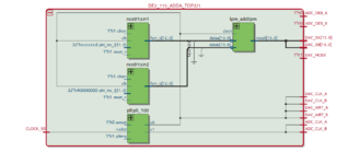
Hello everyone. I am working on a project. I have to send a signal to a card that converts the signal from digital to analog. I found a design diagram of a board similar to the one I have. If you notice the generated signal it enters the DAC. then a loop with sma cable takes the signal to ADC and then it is filtered. I wonder why the fir filter is applied with the input ADC signal. I have always filtered the signal before converting generally.

Screenshot_2022-01-23-01-47-49-329_com.whatsapp.jpg
 

Because a 20 pole digital filer is a whole lot cheaper than an analog one. maybe it’s decimating? There are a lot of reasons to use a digital filter.
 

Hi,

One should always place an analog filter in front of an ADC, acting as anti aliasing filter.
It should attenuate at least all frequencies above f_sample/2. This is above the "frequency of interest",
and makes the digital values clean and reliable.

On the digital side hen you are free to design any filter you want.
Digital filters are
* free (no part cost)
* stable, don't suffer from thermal drift (frequency, DC offset)
* accurate, don't suffer from part tolerances
* predictable
* flexible in type and order
* simple to modify (configuration, software update), no soldering

Klaus
 

It's a demonstration design to make the very first digital signal processing steps. Purpose of the FIR in the specific case is extracting the 1 MHz wave.
 

ok, since it is the project of another AD / DA card different from mine, I imagine that Terasic does this for all of them.
What do you recommend?
in the verilog project I have a signal called ADC_DB and another equal ADC_DA which represent the digital signal output.
They are two identical signals.


With an SMA cable, I convert digital to analog and the ADC converts back to digital.
Where should I put the FIR filter?

I am relying on this example which I have been told is valid.


I have attached the sample card project.
If I wanted to follow the example, I would have to connect the FIR module to ADC_DA (this is the signal of the ADC)
If I wanted to avoid following the example and put the filter first I would have to connect the filter to DAC_DA and then create the loop. (in the project a loop is required that carries the input signal).

the problem that the adc and dac are 14 bits, and the filter has a 27 bits output
 

Attachments

  • Immagine 2022-01-08 180925.png
    Immagine 2022-01-08 180925.png
    29.8 KB · Views: 197

Putting the filter before the DAC doesn’t make a lot of sense. The fact that the filter output is 27 bits is not a “problem”. Simply truncate the output.
 

Status
Not open for further replies.

Similar threads

Part and Inventory Search

Welcome to EDABoard.com

Sponsor

Back
Top