Smillsey
Member level 5
Hi guys
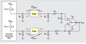
I am designing the output low pass image filter for a DAC that will be generating up to 75MHz sinusoids....
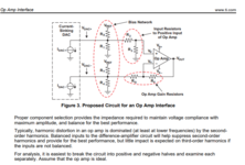
I needed DC coupling so i used this great app note to design the output circuit; https://www.ti.com/lit/an/slyt368/slyt368.pdf
There is a circuit with a filter and a circuit without a filter... but not much info about the filter design itself... I am waiting information from the FPGA engineer about the exact sample rate we will use in order to determine the roll off of the filter...
But my question is where would you put the filter?
See attached the circuits used thus far, I was thinking about just strapping on another op amp after the single ended conversion and implementing an active 2nd order low pass after the existing circuit........ Is there any downside to that?
PS. Ignore the AD8066, i wont be using that specific op amp...
The dac is a 0_20mA complimentary output IC, hence the current sources in the spice below...

I am designing the output low pass image filter for a DAC that will be generating up to 75MHz sinusoids....
I needed DC coupling so i used this great app note to design the output circuit; https://www.ti.com/lit/an/slyt368/slyt368.pdf
There is a circuit with a filter and a circuit without a filter... but not much info about the filter design itself... I am waiting information from the FPGA engineer about the exact sample rate we will use in order to determine the roll off of the filter...
But my question is where would you put the filter?
See attached the circuits used thus far, I was thinking about just strapping on another op amp after the single ended conversion and implementing an active 2nd order low pass after the existing circuit........ Is there any downside to that?
PS. Ignore the AD8066, i wont be using that specific op amp...
The dac is a 0_20mA complimentary output IC, hence the current sources in the spice below...
")