Continue to Site

Welcome to EDAboard.com

Welcome to our site! EDAboard.com is an international Electronics Discussion Forum focused on EDA software, circuits, schematics, books, theory, papers, asic, pld, 8051, DSP, Network, RF, Analog Design, PCB, Service Manuals... and a whole lot more! To participate you need to register. Registration is free. Click here to register now.

[SOLVED] D Flip Flop frequency divider

Status
Not open for further replies.

livecf

Newbie level 5
Newbie level 5
Joined
Apr 7, 2022
Messages
10
Helped
0
Reputation
0
Reaction score
2
Trophy points
3
Activity points
137
Hi all,

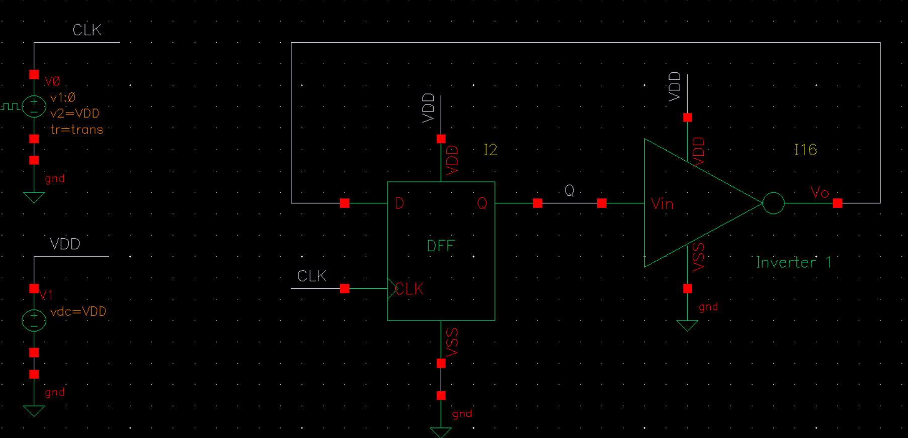
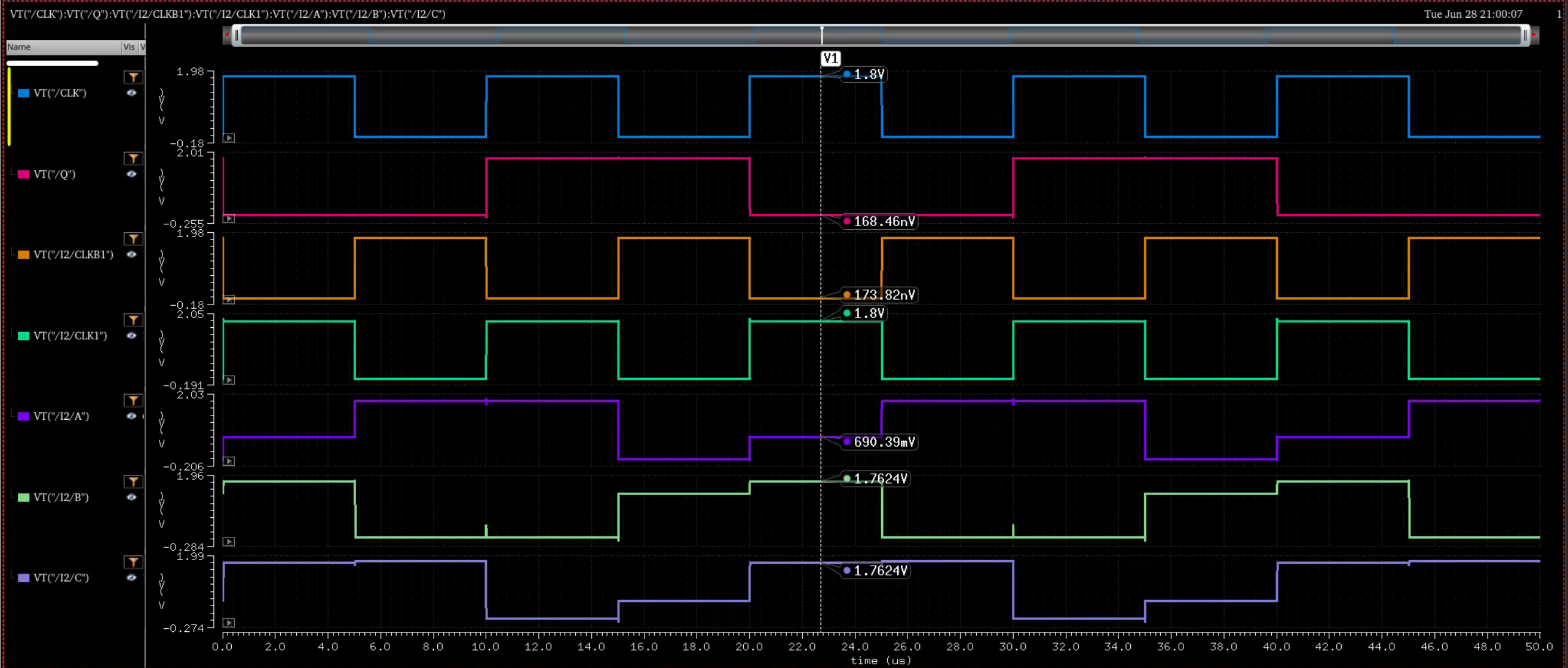
I'm using a transmission gate base DFF to build a simple frequency divider. It worked, but I'm getting some weird waveform at some intermediate nodes and the power consumption is high too (11uW). Could anyone kind enough to provide some insights on this problem.

Here is the testbench, I'm using 1.8V VDD and 100kHz clock.
DFF_tb.png


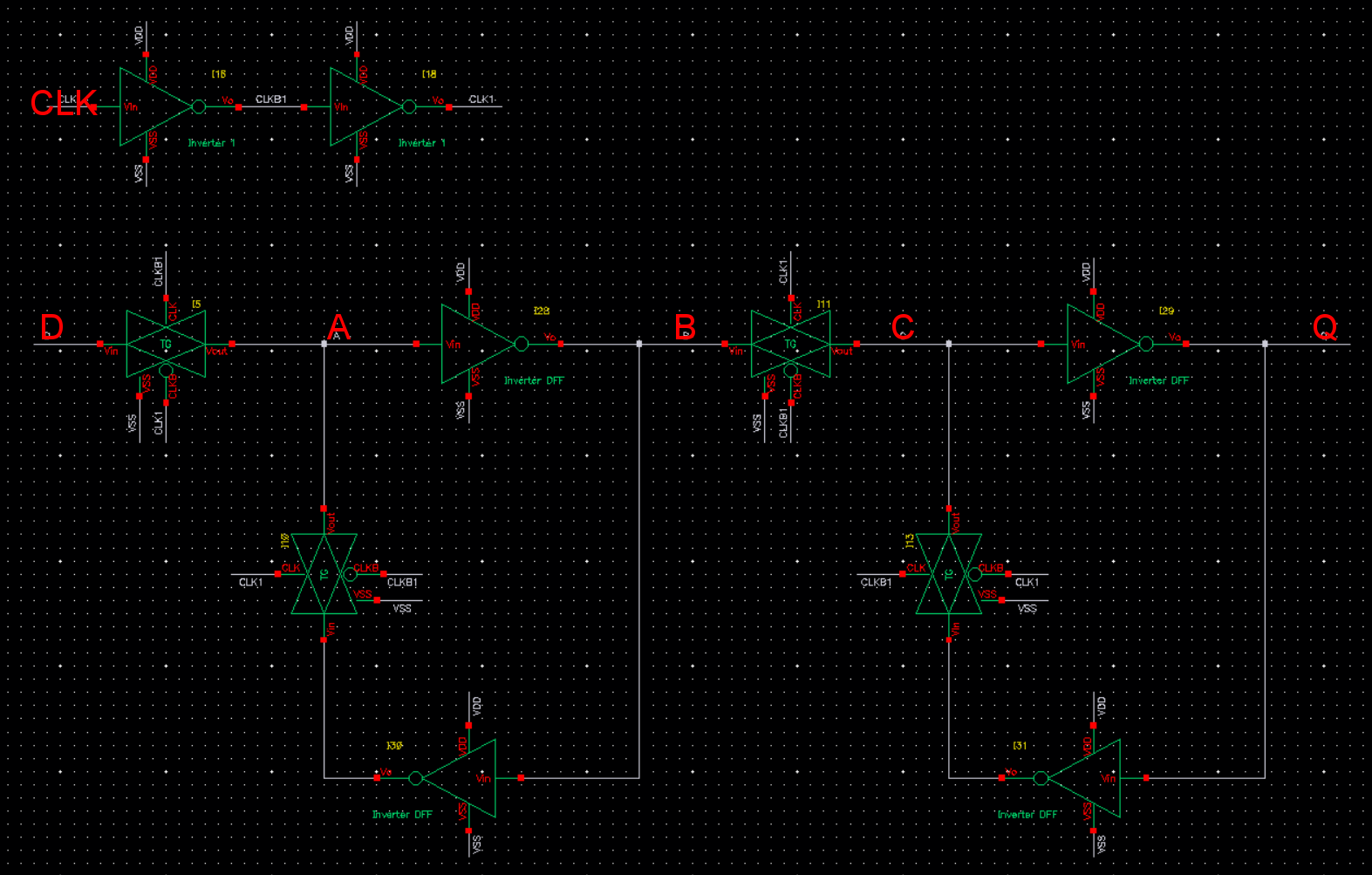
Here is the DFF sch:
DFF.png


Here is the waveform, you can see I have some weird staircase like waves in some nodes.
DFF_waveform.png
 

Solution
well, the problem is that you connected pmos bulk to its drain I think.
usually transmission gate bulks are connected to VSS (nmos) and VDD (pmos), otherwise you cannot really open them. connect m0 bulk to VDD.
how the transmission gates look like? It seems I10 is not closed and/or I5 provides strong DC output current somehow which raise node A's potential
 

Hi,

I´m not familiar with IC design.
But the diagram looks like nodes A, B and C are short circuited somehow.

Also from the DFF schematic it looks like at least nodes A and C can be (are) driven by 2 sources. This calls for trouble.

Klaus
 

well, the problem is that you connected pmos bulk to its drain I think.
usually transmission gate bulks are connected to VSS (nmos) and VDD (pmos), otherwise you cannot really open them. connect m0 bulk to VDD.
 

Solution
well, the problem is that you connected pmos bulk to its drain I think.
usually transmission gate bulks are connected to VSS (nmos) and VDD (pmos), otherwise you cannot really open them. connect m0 bulk to VDD.
Thanks, that solves the problem!
 
Status
Not open for further replies.

Part and Inventory Search

Welcome to EDABoard.com

Sponsor

Back
Top