Continue to Site

Welcome to EDAboard.com

Welcome to our site! EDAboard.com is an international Electronics Discussion Forum focused on EDA software, circuits, schematics, books, theory, papers, asic, pld, 8051, DSP, Network, RF, Analog Design, PCB, Service Manuals... and a whole lot more! To participate you need to register. Registration is free. Click here to register now.

Custom Inductor design .13u Process

Status
Not open for further replies.

ivan848984

Newbie level 4
Joined
Oct 27, 2014
Messages
6
Helped
0
Reputation
0
Reaction score
0
Trophy points
1
Activity points
59
Hello. I am trying to design a custom inductor in Cadence Virtuoso for mm-wave applications in TSMC 130nm. I drew a spiral inductor (as seen in the attachment) in metal 8 and metal 7. I've run Quantus QRC and done RLCk extraction. Y parameter measurement yielded L = 137pH (which matches with theory - Bryan's formula), but Q is pretty high, around 180. I've also modeled inductor in HFSS and got Q = 16.5. I'm guessing I haven't included Substrate extraction in QRC, but I cannot find the techfile for that.
Also, what additional layers should I add in this inductor layout?

Any additional advice about this problem would be extremely helpful.
Thanks.
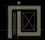
inductor.png substrate.png

Referring to previous thread https://www.edaboard.com/threads/278522/
 
Last edited by a moderator:

Extractions are not generally accurate in these kind of problems.Instead, a EM simulator ( preferably Sonnet or ADS Momentum ) gives more accurate result.
 
There is also a number of electromagnetic simulators specifically designed for integrated inductors, other passive elements, and RF circuits:

- EMX from integrandsoftware.com
- PeakView from lorentzsolution.com
- Veloce... from helic.com
- ...
 
If I undestood correctly, all EM simulators can be linked with Cadence only on schematic level? How do I link/draw them in layout with other components in the layout (mosfets, resistors, capacitors...)? I thought I could draw a spiral which would act as an inductor after RLCk extraction. I have found this document on Cadence's web site, where they did the same thing, but included substrate extraction as well (and got pretty accurate matching after the measurements) which I don't know how to do (there is some "procfile" in the PDK where substrate parameters are listed, but that's all I know).
As I said above, I drew the same inductor in HFSS and got similar inductance as Cadence, but Q factor is different because I didn't select the additional substrate extraction in Cadence (I think) .
There are many ways to do a layout based EM simulation.The best one is to install a Cadence compatible EM simulator. ( Sonnet-Blink is very popular, ADS Momentum is also fine ).Since installation is correct then you will able to create "sonnetview" by using this tool and after that you can simulate this "special view" in Sonnet environment.Then you should import this with its s-parameters and model into your testbench schematic.
Another method is to create DXF or GDSII file of this particular coil layout then import it into any planar EM simulator and simulate it.Then after obtaining s-parameters, you can import this model that is defined by s-parameters onto your schematic by using n-port component.
 
I understand that, but how do I do that in the opposite direction? This is the flow I would need
Cadence layout structure (like the one in the first post) -> Sonnet EM simulation of that structure -> import back layout view with losses and parasitics back into Cadence with other components in the layout. Is this possible and how do I do that? Thanks.
You should create a config view that seperate into your active circuit and coil.Extract your active block without coil and replace your coil with 2pins that get out from extracted block.Then do your Em simulation and connect your s-parameters block coming from EM simulation to these pins.You can also create PI type equivalent model in order to simplify the simulations because PSS like simulator tools don't like piecewise extrapolations.
 
If I undestood correctly, all EM simulators can be linked with Cadence only on schematic level? How do I link/draw them in layout with other components in the layout (mosfets, resistors, capacitors...)? I thought I could draw a spiral which would act as an inductor after RLCk extraction. I have found this document on Cadence's web site, where they did the same thing, but included substrate extraction as well (and got pretty accurate matching after the measurements) which I don't know how to do (there is some "procfile" in the PDK where substrate parameters are listed, but that's all I know).
As I said above, I drew the same inductor in HFSS and got similar inductance as Cadence, but Q factor is different because I didn't select the additional substrate extraction in Cadence (I think) .

Your understanding is absolutely right.
- substrate extraction will give you fairly accurate Q - that will be very close to some EM solvers.
The issue in my experience I faced with few EM solutions in lower nodes - they do not model erosion, loading-effect, RIE (Reactive Ion Etching) as required by fab - in an easy way as QRC ICT does. Some of them we tried & used it in bit complex way. in general these EM solvers are very good for modeling an independent inductor. QRC is not a modeling tool BTW. The goodness that we realized with QRC, is when multiple RF sensitive components placed nearby - mutual interaction from one inductor to the other is captured pretty well - which is lacking in independent model based methodology. However nobody is going to stop a modelling guy to bundle multiple inductors and multi-port complex model - which IMHO is expensive [overall TAT in the flow and integration hassle] - on the contrary, when you are Cadence flow, QRC-RF methodology is much cheaper solution w.r.t. TAT, and much flow-friendly.
For substrate extraction - you've to get doping profiles and substrate files from foundry - sometimes ppl get these through Cadence channel.
 
Status
Not open for further replies.

Part and Inventory Search

Welcome to EDABoard.com

Sponsor

Back
Top