Continue to Site

Welcome to EDAboard.com

Welcome to our site! EDAboard.com is an international Electronics Discussion Forum focused on EDA software, circuits, schematics, books, theory, papers, asic, pld, 8051, DSP, Network, RF, Analog Design, PCB, Service Manuals... and a whole lot more! To participate you need to register. Registration is free. Click here to register now.

current-starved inverter (baker)

Status
Not open for further replies.

zitty

Member level 2
Joined
Aug 2, 2010
Messages
42
Helped
0
Reputation
0
Reaction score
0
Trophy points
1,286
Activity points
1,628
Hello,

I want to design a VCO with current-starved inverters as delay cells.
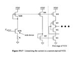
In the baker book they do a linearization of the input current as shown in the picture in the attachment.

M3 and M2 are sized with minimum l and w3/w2=2.
M4 and M1 work as current sources and they control the current flowing in the inverter.

I want to oscillate the VCO with a certain frequency fosc at Vdd/2. And I calculated the necessary current to achieve this frequency with the formula given in the book.

fosc=1/(N*2*td)=Id/(N*Ctot*Vdd)
where:
N=number of stages
td=inverter delay
Id= drain current of M4 and the others
Ctot=Cout+Cin=total capacitance on the drains of M2 and M3

Now I want to use the linearization circuit consistion of M5R, M6R, R and M5 and M6 to achieve a linear relation between Vin_VCO and this current.

M6 has the same sizes as M4 and M5 has the same sizes as M1.
MR6 and M5R are quite wide.

Now my problem. When I generate a current Id_M6R it will be mirrored into M6 and M4 right?

but how do I have to choose the transistorsizes that I will end up with the current that is necessary for the desired frequency fvco?

It seems that Id6 is not equal to Id4 any more because of the degradation of the drain voltages in M1 and M2? but I dont understand how this should work?

thanks for helping
 

Attachments

  • vco1.jpg
    vco1.jpg
    42.1 KB · Views: 349

These are only three current mirrors: the linearization is achieved by using a wide M5R so its Vgs~Vth hence (neglecting body effect): the voltage across the resistor in the source of M5R is VinVCO-Vth and the branch current is (almost) linear
I=(VinVCO-Vth)/R
If you have problems mirroring accurately you should still be able to increase L to reduce Early effect: if this is not an option (too slow) then you need to use a regulated mirror... see next chapter in Baker's book (at least in the 2nd edition)
 

But how do I have to dimension theese current mirrors?
I chose equal sizes for the transistors on top and for the resistors on the bottom so that
W4/l4=w6/l6 and w1/l1=w5/l5.
But the current there was not the same. I measured the average current in the inverter and the current in the operating point through the biasing branch.
 

... the current there was not the same.

Ids vs. Vgs curves are not horizontal, i.e. Ids also depends on Vds. The Vds voltage levels differ.
 

zitty can you give us the currents in the M6R M6 and M4 branch?
The current for the M4 branch would be the current when M3 switch is active (and settled)
You should be able to flatten your Ids vs Vgs curves (hence increase current matching) by increasing the length of M6R M6 M4 M5 M1
 

hello,

ok i measured the currents now. They are about:
I_Mr6=10uA
I_M6=7uA
I_M4=5uA
I use long channel devices for all the pmos transistors on top of the circuit.

Another question: how good can the linearization with this technique be?
I mean: is the transfer characteristic of the VCO linear if the current is a linear function of the input voltage?
are there other things to regard?
 

Assuming all your devices are in saturation (did you check?) , you need to increase the L of M6R M6 M4 until you get some current matching between M6R and M6.

If this is not enough then you need to find another way to decrease Early effect: examples include
- cascoding (very effective)
- source degeneration
- GD resistors (poor for matching but it might be ok depending on process)

As of how good this will be, it depends on how much body effect you have on your wide NFET because its Vth is not a constant but a function of the source voltage (and hence of the current itself): this contributes a nonlinear term in the I(Vin) relation. You can easily write the SPICE level 1 equation to have an estimate
 

i achieved a better current matching between Id_M6R and Id_M6 with cascoding.
but i´m still not able to mirror this current into the inverter branches.(Id_M4)
cascoding is not possible here because this reduces the voltage swing of the inverter.

how could i mirror this biasing current into the inverter?
i mean every linearization does not help when i´m not able to mirror this linearized current into my inverter chain.

would it be better to bias the gates of M4 and M1 in an other way?
 

if it worked for M6 and M6R there is no reason why it would not work for the M4 branch; you can always reduce the vdsat (yes at some point it will impact current matching) of the cascoded pairs to make it as large as as the single-device current source:
as long as your output is keeping either PMOS or NMOS cascode pair in saturation you will slew at constant current once the cascode device is pushed into linear you will still slew with poorer control but you should still get to the rail, right? Even if you were not to reach the rails you can still create a ring oscillator with a smaller swing and still meet your specs.
Let us know if this does not work for you and indicate what process/voltage you are using.
 

i´m not sure wheater i understand.

because i had problems with the current matching i designed my mirroring circuit in a way that the pmos (M6 M6R ) and nmos tranistors (M5) are in saturation over a wide range of my input voltage variation (gnd to vdd). this had been my main design issue for this part.

i work with a cascode current mirror (wide swing) within the biasing branches (M6 and M6R) to achive better current matching. therfor will have to do this also in the branch with the inverters. therefor i have 6 transisors stacked on top of each other in the inverter branch.

i thought transistors M4 and M1 should operate as resistors to limit the current in the inverters. as far as i understood this will also be the case within a cascode current mirror.

now when i connect my mirring circuit (where i have the same current in each branch) with determinde transistor ratios to my current-starved inverter branch i get a dc current at the switching point as well as average current. i think thats because of the resistance of the inverter devices (M2 and M3) that lead to a different vds of M1 compared to M5 and M4 compared to M6. Where K1=K5 and K4=K6. anyhow i was not able to mirror the current out of my biasing circuit into the inverter stage.
But i have at least 100mV overdrive for M1 and M4 as well as the cascoded devices.

what did you mean with the vdsat? can you give me an example?
 

Hi zitty
I am in a bit of a rush now but M4 and M1 being current mirrors have to be in saturation not in linear (resistor) region that is how current in controlled; M2 and M3 act as switches hence they operate in linear.
Vdsat is the minimum Vds that keeps the device in saturation
I will re-read your post later to see if I left anything out
 
  • Like
Reactions: zitty

    zitty

    Points: 2
    Helpful Answer Positive Rating
thanks for your help dgnani.
i think i understand now. i read again through "the designers guide to jitter in ringsocillators". there they propose both solutions.
once with the controlling devices in saturation and once in linear region.

because my devices were in linear region by itself i thought that would be the correct way.
its not so easy to force them to operate as current sources.
 

can you guys make this current starved VCO working at desired frequency range, i tried to use this one for 100M~500MHz in 130nm CMOS process, it doesn't cover the frequency range in any case.
anyone has the experience in this topology for wide tuning range? actually 100M~500MHz is not that wide at all.
 

Status
Not open for further replies.

Part and Inventory Search

Welcome to EDABoard.com

Sponsor

Back
Top