Continue to Site

Welcome to EDAboard.com

Welcome to our site! EDAboard.com is an international Electronics Discussion Forum focused on EDA software, circuits, schematics, books, theory, papers, asic, pld, 8051, DSP, Network, RF, Analog Design, PCB, Service Manuals... and a whole lot more! To participate you need to register. Registration is free. Click here to register now.

[SOLVED] Current sense resistor for SMPS?

Status
Not open for further replies.

bowman1710

Full Member level 3
Joined
Nov 8, 2014
Messages
183
Helped
6
Reputation
12
Reaction score
6
Trophy points
18
Activity points
1,604
Hi Guys,

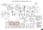
Quick question about this schematic

Looking at the CS signal, for the LTC3723. How have they chosen 15mOhm total resistance for the current sense signal? How i see it is that the device has a limit of 280mV with that being so, 280mV/15mOhm=18A or so. I haven't done a lot of current sense work so I guess that duty cycle will effect it but cant see any stuff on-line about choosing the right value apart from what I have done above. But if that is how you do it, why does it work out to around 18A when at most the primary will be 6-7A or so?
push-pull.PNG
 

The NORMAL input current might only be six or seven amps, but think about what might possibly go wrong in the hands of an idiot....

Very high, or very low input voltages, extremes of input duty cycle, abuse of the output.
The designer has added several features to try to make it as indestructible as possible, and he probably worked out that the bridge driver mosfets could be protected with a very fast 18 Amp current limit.

Its not really there to do much during normal operation, it a safety feature of last resort to prevent destruction if things somehow go very wrong.
 

Agreed with everything above. Allowing the max input current to swing far above the steady state current allows for faster transient response. Also a lower sense resistance gives less dissipation. On the other hand, your current sense signal will be more susceptible to EMI and false triggering. But there's not really an exact method for selecting an optimal sense resistor value.
 

Fine that seems to make sense, just another quick question on it. What is the best way to determine the optimum output inductor needed on the secondary for this design?
 

IC Current shunt sensors are typically 75mV or 100mV max drop for low loss and adequate resolution. But some leeway is possible.

Choke selection is a tradeoff between saturation current for suitable size/cost and attenuation of ripple with impedance ratio of ZL/Zc, which includes ESR ( or Rs). TDK make best choices. Or cost vs ripple to input and outputs.
 

another quick question on it. What is the best way to determine the optimum output inductor needed on the secondary for this design?
The output voltage is relatively low, and the dc current relatively high.
The ratio of ac (small) to dc current (high) implies the use of a low cost powdered iron toroid might be ideal.
As the required inductance is very low, only a very few turns will be needed.

Check out the Micrometals website, they have some easy to use free design software which will give you a range of solutions to choose between.
**broken link removed**
 

Choke selection is a tradeoff between saturation current for suitable size/cost and attenuation of ripple with impedance ratio of ZL/Zc, which includes ESR ( or Rs). TDK make best choices. Or cost vs ripple to input and outputs.

As the required inductance is very low, only a very few turns will be needed.

Basically I have a 50V input on the transformer and I need 350 rectified on the output, I have a 1:7 transformer. If i know the switching frequency etc what calculations do I need to work out the ideal size but I get like 100uH and cant work out whether that is in the right ball park figure or not?
 

Basically I have a 50V input on the transformer and I need 350 rectified on the output, I have a 1:7 transformer. If i know the switching frequency etc what calculations do I need to work out the ideal size but I get like 100uH and cant work out whether that is in the right ball park figure or not?
Ah !
The schematic you showed in your first post showed an output of 12v at 20 Amps.
This has all suddenly become very different !

O/k so we now have 350 rectified dc volts, but at what current ?
And what is the switching frequency ?
And what is the min/max dc input voltage range you anticipate ?
It all matters.
 

Ok

The controller switching frequency is 333KHz so transfomer switching frequency is 166.5Khz roughly. Its 350V @ 200W output 0.57A. The min and max is 40-60V at the input. Yes I had a feeling it did all matter but I couldn't see in what way, or the correct way, like I said I have tried to work it out but wasn't sure on my answer.
 

Taking the minimum input voltage of 40v, we need to allow for conduction losses and voltage drops everywhere, to get 350 dc volts at something like 95 % maximum duty cycle at the output of the rectifier (allowing for 5% dead time).

In practice the transformer may need to have a ratio more like 35v to 370v to run at full power with only 40v input.
So a 7:1 transformer is not going to have enough voltage step up at minimum input volts.

At 60v input, the duty cycle will pull back to about 2/3 of 95% say 63%
and the peak voltage coming out of the rectifiers might be up around 555 volts (but with only a 63% duty cycle) giving 350 volts averaged dc output.

The input to the choke is going to be 0v and 555v alternately at one end, (changing at twice the switching frequency) and fixed 350 dc at the other end.
The average ac voltage across the choke worst case would be half of 555 or 278 volts at 50% duty cycle. It will never quite get down to 50% duty cycle, but that would be the worst case.

From that, we decide what our maximum ripple current is going to be, lets assume 30% of 200mA or 60mA peak to peak.

We need an inductor that will ramp 60mA in 3uS with 278 volts across it. L = 278 volts x 3uS divided by 0.06A
That comes out at 13.9mH
Max peak current will be 230mA

There are a lot of rather wild assumptions being made here, and you may decide on a lower ripple current or change and refine a few things. But something around 14mH to 20mH would probably be sufficient.

It will need to have enough turns to support 278 volts for 3uS, and an air gap that will safely support more than 260mA.
 

Cheers Tony,

In practice the transformer may need to have a ratio more like 35v to 370v to run at full power with only 40v input.
So a 7:1 transformer is not going to have enough voltage step up at minimum input volts.

The design it made so that the output will drop below 50V with the duty cycle being fixed at max.

At 60v input, the duty cycle will pull back to about 2/3 of 95% say 63%
and the peak voltage coming out of the rectifiers might be up around 555 volts (but with only a 63% duty cycle) giving 350 volts averaged dc output.

Wouldnt at 60V Vin wouldn't it be 60x7=420V........420V/350V=83% duty cycle?

lets assume 30% of 200mA

why 200mA?
 

The design it made so that the output will drop below 50V with the duty cycle being fixed at max.

O/k I did not know that, I just assumed you wanted full power right down to the 40v minimum input.

Wouldn’t at 60V Vin wouldn't it be 60x7=420V........420V/350V=83% duty cycle?

Yes you are quite right.
But you still need to think about voltage drops around the system at full power. You will never achieve a full 7:1 voltage step up at full power taken from the dc input voltage, it will be less than that.

why 200mA?

My mistake, I confused 200 watts output with 200mA output.
It will obviously be 570mA output at 350 volts.

- - - Updated - - -

In the new situation, the voltage across the choke with 420 volts at the secondary will be:
83% conduction, 2.49uS, with 70 v across the choke (420v-350v)
17% non conduction, 0.51uS , with 350v across the choke.
Same volt microseconds each way.

570mA dc output, let's make peak to peak ripple 170mA
L = 70v x 2.49uS divided by 0.177 A
L = 985uH
 
Last edited:
570mA dc output, let's make peak to peak ripple 170mA
L = 70v x 2.49uS divided by 0.177 A
L = 985uH

Yes, ok then that is what I have got/been looking at 1000uH (sorry typo in post 7), but I couldn't work out whether that was right because when I look at my slope resistor for the controller it doesn't really work out at a high voltage for a high secondary inductor.

Given that:

Equation.PNG

Is why i thought I had gone wrong unless i'm using the wrong way of calculating the slope resistor

With:

Vsec=350v
Lsec=1000uH
Ns/Np=7
Rsense=0.015ohm
 
Last edited:

The current ramp is difficult to anticipate, but very easy to measure.

All you need is to add enough slope compensation to double the amplitude plus a little bit extra.
That will guarantee stability.

If you add too much, I have read that you begin to lose some of the advantages of current mode control.
The "real" current ramp gets swamped (buried) by the added slope compensation.
This effects the inner current control loop, and the whole system begins to dynamically revert to just having the outer voltage control loop.

I usually fit a potentiometer so I can set the slope compensation to zero. Load it all up and monitor the real current ramp, then tweak the potentiometer up for exactly twice the amplitude.
 
I usually fit a potentiometer so I can set the slope compensation to zero. Load it all up and monitor the real current ramp, then tweak the potentiometer up for exactly twice the amplitude.

How would you go about for the calculations for the other resistor and C as highlighted below then?

Slope compensation.PNG
 

The 75K and 470R voltage divider just adds a pretty constant 31mV on top of the shunt voltage.
Too lazy to look up the data on the control chip, but the current limit pin probably trips some kind of shutdown mechanism at a set threshold.

The original designer decided to add 31mV to the shunt voltage, probably because he had to use commonly available resistor values for his shunt, and the internal current limit voltage threshold of the chip is fixed.

So as a fine tuning mechanism he arranged for the current limit to trip at the exact current he wanted, by adding a constant 31mV.

The 330pF capacitor and 470R resistor act as a fast integrator to knock any leading edge spike off the current waveform.
This spike can arise from parasitic inductance in the source circuit, and more likely from direct capacitive gate/source coupling when the gate driver chip switches on the gate. This can produce a very short voltage spike that might cause false current tripping.

It is not something to calculate, just monitor the current waveform at pin 10, and experimentally fit just enough capacitance to knock the spike off the leading edge, but no more.

All these components are just a bit of selective tweaking by the designer to get everything working really well during the final stages of prototype testing.
 
Thank you so much warspeed for your help it has been invaluable hopefully I shall be able to progress forward with this and work something out that will help with my prototype design. Once again thanks.
 

Status
Not open for further replies.

Similar threads

Part and Inventory Search

Welcome to EDABoard.com

Sponsor

Back
Top