Continue to Site

Welcome to EDAboard.com

Welcome to our site! EDAboard.com is an international Electronics Discussion Forum focused on EDA software, circuits, schematics, books, theory, papers, asic, pld, 8051, DSP, Network, RF, Analog Design, PCB, Service Manuals... and a whole lot more! To participate you need to register. Registration is free. Click here to register now.

current mirror for bias circuit

Status
Not open for further replies.

crazyfox

Junior Member level 2
Joined
May 12, 2007
Messages
23
Helped
0
Reputation
0
Reaction score
0
Trophy points
1,281
Activity points
1,452
need for start up circuit in beta multiplier
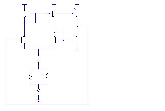
HI:

I have got a circuit like below , it was a current mirror used for bias

The problem is that i have never seen a circuit like this

Anyone who has ever seen the topology like this , pleas give me a help

THX!


The circuit is a kind of self-biased topology. I'll try to explain the way I understand it. Look at the attached picture. In Fig.1 I have redrawn your original circuit in a slightly different way. The part in the dashed line box is a well-known structure used in bandgaps with bjt or delta Vgs based current sources with CMOS or even band-gaps with CMOS if M1 and M2 are in subthreshold. I assume that W/L of M1 is bigger than W/L of M2 so that you can have VR+Vgs1=Vgs2 for the same amount of current through M1 and M2. Which means that W/L of M5 is the same as that of M6.
As usual for these kind of circuits, the zero current state in all branches is a perfectly stable state, so you need a start-up circuit. But let's see what happens if we manage to kick the circuit out of this zero current state. If the current through M3 is small (and it gets mirrored in M5 and M6) then the drop across the resistor is almost nothing, which is as if the source of M1 is at ground. In this situation M2 is in cut-off or thereabout because its W/L is smaller than that of M1 and if the current of M1 is small, that of M2 should be even smaller. Voltage V1 should be high, or going higher if we assume that initially it was 0v and M6 is charging all the caps attached to that node. As it goes high M3 starts conducting more and more current which increases the drop across the resistor and also the gate voltage of M1, which in its turn increases the current through M2. Now, if you imagine for a moment that we somehow decouple the current of M6 from that of the M2 and we design the PMOS mirror such that PMOS currents increase slower with V1 than the current of M2 (something similar to what is on Fig.2) then for some V1 the two current curves will intercept and this will be another stable point at which the circuit will settle. The feedback will try to maintain it.
 

sutapanaki made a well job. but what is the advantage of this bias comparing to others.
 

According to me it has all the benefits of the so called beta-multiplier bias - good independence of Vdd, fixing the gm of other biased transistors to be proportional to 1/R and should have the same temperature behavior as that of the beta-multiplier. The different thing here is that the two NMOS transistors, M1 and M2 have the same drain voltages, if of course M3 is in ratio to them.
 

Status
Not open for further replies.

Similar threads

Part and Inventory Search

Welcome to EDABoard.com

Sponsor

Back
Top