Continue to Site

Welcome to EDAboard.com

Welcome to our site! EDAboard.com is an international Electronics Discussion Forum focused on EDA software, circuits, schematics, books, theory, papers, asic, pld, 8051, DSP, Network, RF, Analog Design, PCB, Service Manuals... and a whole lot more! To participate you need to register. Registration is free. Click here to register now.

Current Mirror Differential Amplifier Layout Matching using Cadence

Status
Not open for further replies.

bluesy

Junior Member level 1
Joined
Jan 12, 2011
Messages
18
Helped
0
Reputation
0
Reaction score
0
Trophy points
1,281
Activity points
1,416
Hihi, may i know how to do interdigitize?? i have inserted two transistors one by one into layout . how should i do so that i can digitize both transistors together for matching? may i know that do i need to do modifications like adding transistor or others on my schematic? or i just need to leave schematic there having two transistors only for the current mirror? between, if my sizing of current mirror is 1:10 , can i use interdigitize or what should i do for the matching purpose?

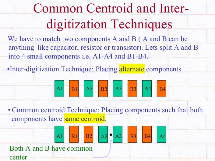
For diffential amplifier, is that the best way is using common centriod? may i know how to fo the connection between them in schematic and layout as well. Besides, how should i do the sizing? For example, the total width two transistors of differential amplifier in my design is 20u each and i have fingered into 2 for the layout. Do i still need to do common centroid? If yes, how i do sizing for the transistors if i split the transistors to 4 instead of 2.
i am planning to do the matching as below:
A1 B1
B2 A2


thank you so much for your help
 

for the current mirror you can use a multiplicity greater than 1 for the minimum transistor, i.e. 2:2 instead of 1:1 and use for example ABAB. If you have 1:10 it is of course a bit more complicated and boring. You can always increase the minimum and put fingers between those of the other transistor.

For diffamps, yes, common centroid is the best. In case that you need very good matchin performances you should use it. However, in case offset is not a major concern, you can ignore it and use simpler simmetries. The mosfet sizing depends on all of the design specifications, gain, noise, speed, bias, and yes, offset. Remember that offset is proportional to 1 over the square root of the MOS area, fingered or not.

Your way of doing common centroid is good. You can also bring it to the extreme using something like that:
MOS 20x1 (for example) you can divide it into 4 MOS 5x1 so that u have A1B1C1D1 and A2B2C2D2. You can put it like that:

A1B1 C1D1
C2D2 A2B2

or

A1A2 C1C2
D1D2 B1B2

there are a lot of ways of combining common centroid, simmetry and interdigitation. However, in my opinion, it is not always useful. The layout should be made with care that increase with the required offset permormance. If your amplifier should have by design 10 mV offset, just do simple common centroid or simple simmetry, size properly the area, and that's enough.
Check the book "Art of Analog Layout" from Alan Hastings for details.
 
  • Like
Reactions: bluesy

    bluesy

    Points: 2
    Helpful Answer Positive Rating
Common centroid is a good practice. You should also keep in mind that splitting a 20x1 MOS into 4, 5x1MOS can have some effect on your simulation. it is better to double check.
You should also try to maintain symmetry in your connectivity.
 
  • Like
Reactions: bluesy

    bluesy

    Points: 2
    Helpful Answer Positive Rating
I suggest you to do "common centroid" method instead,, if you are to layout a differential pair. The topology is quiet simple :

M1 M2 M2 M1 M1 M2 M2 M1 M1 M2 M2 M1

You can extend it as much and as appropriate as possible, depending on the size of transistors you want to design.
Hope this helps.
For more clarity, you can take a look at this picture. credit to original maker.
 
  • Like
Reactions: bluesy

    bluesy

    Points: 2
    Helpful Answer Positive Rating
Thank you so much :smile: , but may i know that i is that i need to redraw the schematic in order to pass the LVS. For example , i have 20u transistor and i splitting them into 4, is that i need to make changes in my schematic then only i can do matching in the layout?
 

It depends on your PDK. In some PDKs you can set the number of fingers (NF) and the multiplicity (M) in others you need to insert M 2-finger transistors.
 
  • Like
Reactions: bluesy

    bluesy

    Points: 2
    Helpful Answer Positive Rating
I see, is that i want to split it into 4,then i just put multiplier 4 then proceed to layout? thank you so much :smile:
 

Status
Not open for further replies.

Part and Inventory Search

Welcome to EDABoard.com

Sponsor

Back
Top