Continue to Site

Welcome to EDAboard.com

Welcome to our site! EDAboard.com is an international Electronics Discussion Forum focused on EDA software, circuits, schematics, books, theory, papers, asic, pld, 8051, DSP, Network, RF, Analog Design, PCB, Service Manuals... and a whole lot more! To participate you need to register. Registration is free. Click here to register now.

current limiter overshoot

Status
Not open for further replies.

keevvee

Newbie level 6
Newbie level 6
Joined
Feb 7, 2014
Messages
11
Helped
0
Reputation
0
Reaction score
0
Trophy points
1
Location
Norway
Visit site
Activity points
108
Dear all,

I'm struggling with an existing current limiter that looks like this:
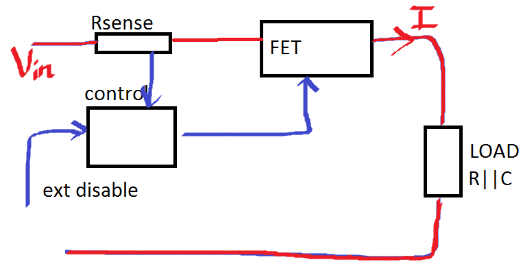
7221067800_1391802717.png


The problem I have is when Vin applied rapidly (high dv/dt) a current peak sneaks through.
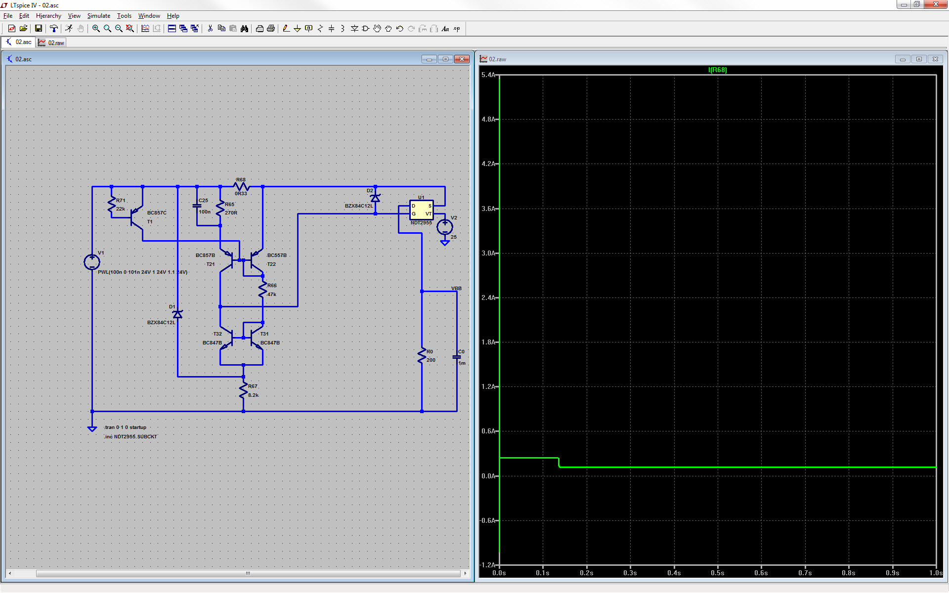
7315269700_1391802722.jpg


The meas & control is designed so the FET is OFF as long as the current is above the threshold, this is not a latching limiter, it's an analogue and I have exterminated the control circuit. No problem it's following from the first picosends. My theory is the FET capacitance (D-S), like this:
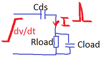
6662180000_1391802717.png


I even made a simulation in which the FET always biased OFF and the current peak is still present.
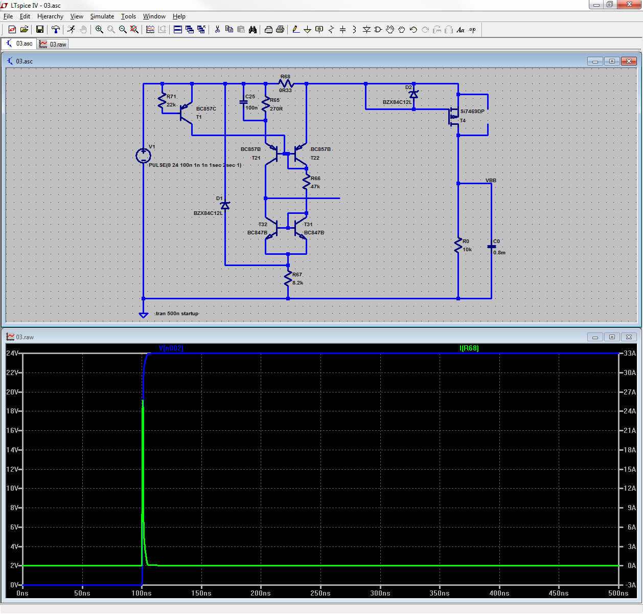
6855854600_1391802715.jpg


Furthermore I have added a CAP in parallel to the FET and the current peak was higher.
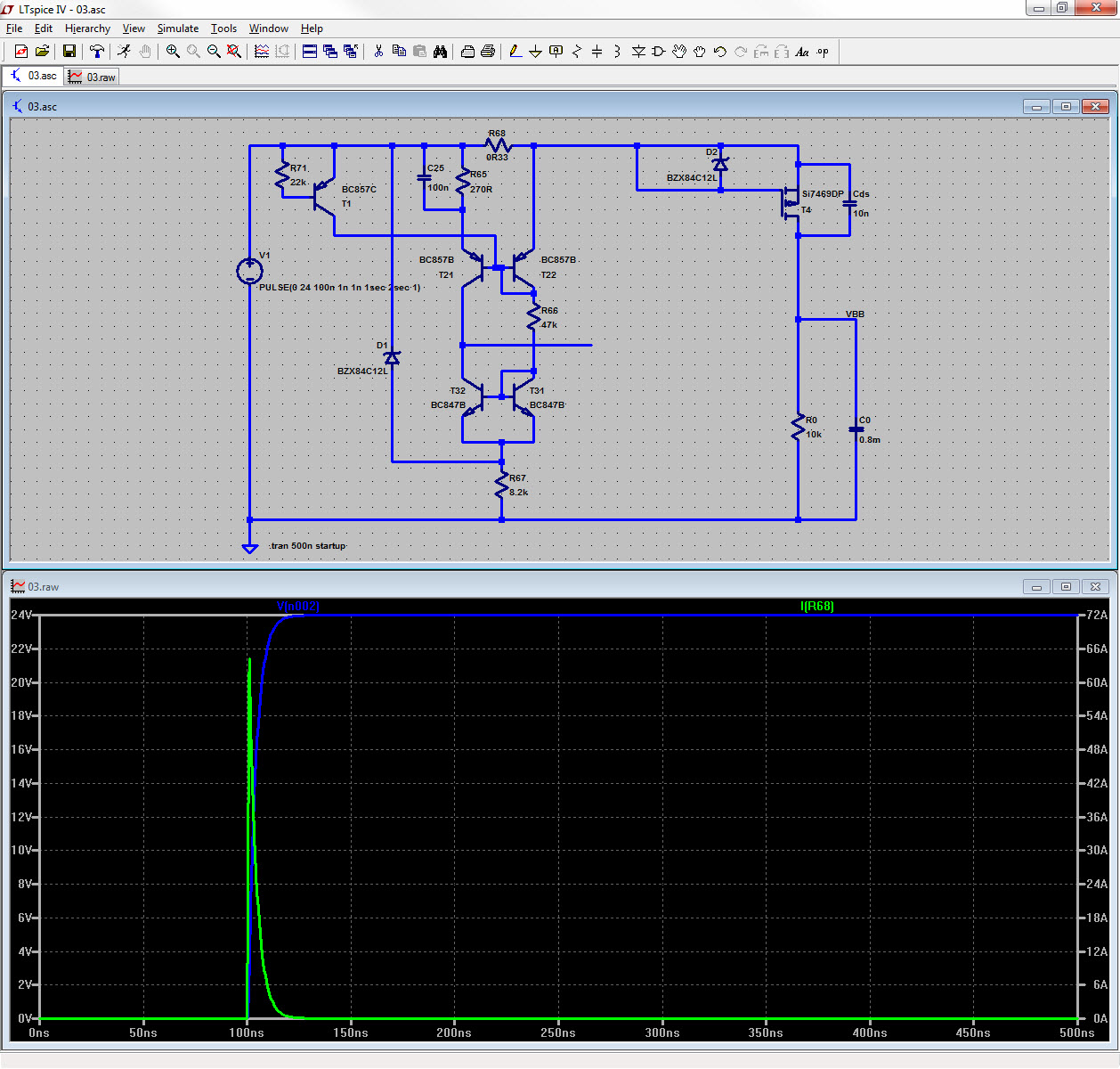
2814607900_1391802720.jpg


After this short transient, the current limiter is working properly, limiting the current until the Cload is charged.

Do you agree with my analysis?
Is there anything to removed the transient current in the first nanoseconds?
I know a nice circuit would be a one that has a RES limiting the current by default and then switching after the power on to a direct conn. but the circuit it already in market and I'm wondering how to reduce the problem with minimum effort.

Thank you in advance.
 

The assumed voltage ns rise times are unrealistic for most voltage sources. Do you have any reason to assume that fast voltage edges and high current capability of the source? What's the application?

Technically the current spikes are simply representing the MOSFET output capacitance. It's strongly nonlinear and the total drain-source charge is considerably higher than expectable from the output capacitance measured at -40 V. Using a FET with less output capacitance is the only way to reduce the spike, if applicable. As a first step, assume realistic voltage rise times.
 
I agree with FvM that 1ns rise and fall times for your source seems unrealistic. That implies a frequency response of at least several hundred MHz. What is the source in actuality?
 

Hi guys, thanks for posting!

This is a part of a device connected in industrial installations, where power supply is 24 V DC.

Don't know standards that applies to it but I'm making some functional tests and in the spec. which I've got the current limit is poorly defined, simply that "the device has a built-in current limiter < 250 mA and the current limiter shall be tested by rapidly connecting the power"

I'm using TTi CPX power supply with an output enable button and the power on response is fast enough to generate a current peak of about 5A, right after that it's limiting nicely to 220 mA and then power consumption drops to idle state 80 mA.

After I saw this 5A super short peak I've simulated the current limiter and findings you know.
If I change the rise time to 0.5us in the simulation the peak will be like 3.3A.

Now depends on how strict my interpretation is going to be, because 5A peak (even very short) does not comply with limit < 250 mA ..

09-02-2014 15-48-57.jpginrush.pngzoomed.jpg
 

You didn't tell what's actual voltage rise time of the said bench top supply. In so far the measurements can't be related to the simualtions. I also don't see 5A peak in one of your real measurements, maybe I didn't understand it right.

But apart from considerations about realistic supply voltage waveforms. If you assume unusally fast voltage rise and respective current peaks generated just by transistor capcitances, you may want an additional short switch. It will however need a gate voltage source to turn it on from the start.
 
Last edited:

The screen dumps from Agilent: PURPLE color is the power supply Vout, the GREEN is the current measured across a 1 Ohm RES in series with DUT.
On the first picture you see the narrow high current peak (going outside the screen, indicated with red arrow), then current limiting period and drop to some kind of normal consumption. The second picture is zommed on the narrow peak, showing the Vout (purple) rise time -in this case <10us (but I will measure at next occasion) and the related current peak (the measured max 4.8 V is in fact 4.8 A).
 

You show a 10k ohm load. Is that a typical load for this circuit?

Here are two options:

Add an inductor in series to slow the input rise-time. But it may not be desirable to have an inductor in series with the load.

Add a larger capacitor across the load to absorb the initial transient current.
 

10 us risetime is "a bit more" than the ns in your initial simulation. It won't generate a 5A current spike through the MOSFET Cds. If you see a spike of this amount, we can assume that the transistor isn't properly switched off.
 
My simulation shows a 4.2A peak current for a 10ns, 24V pulse input driving the P-MOSFET source and gate tied together with the drain grounded. For a 10µs pulse I got a 7.4mA peak current.
 
  • Like
Reactions: FvM and keevvee

    keevvee

    Points: 2
    Helpful Answer Positive Rating

    FvM

    Points: 2
    Helpful Answer Positive Rating
I confirm your simulation:
4.2 A @ 10 ns rise and MOSFET gate tied to source
7.4 mA @ 10us rise and MOSFET gate tied to source

done two more:
129 mA @ 0.5us rise and MOSFET gate tied to source
----------------------
3.3A @ 0.5us rise if connected to control circuit

Sound like you're right. Perhaps it's not properly switched ON.

The LT Spice netlist is here:
Code:
Version 4
SHEET 1 1236 852
WIRE -320 -160 -400 -160
WIRE -192 -160 -320 -160
WIRE -48 -160 -192 -160
WIRE 32 -160 -48 -160
WIRE 128 -160 32 -160
WIRE 176 -160 128 -160
WIRE 304 -160 256 -160
WIRE 496 -160 304 -160
WIRE 768 -160 496 -160
WIRE 960 -160 768 -160
WIRE 768 -144 768 -160
WIRE -320 -128 -320 -160
WIRE 32 -112 32 -160
WIRE 128 -112 128 -160
WIRE -192 -80 -192 -160
WIRE 960 -64 960 -160
WIRE 768 -48 768 -80
WIRE 768 -48 448 -48
WIRE 912 -48 768 -48
WIRE -320 -32 -320 -48
WIRE -256 -32 -320 -32
WIRE 32 0 32 -48
WIRE 128 0 128 -32
WIRE 128 0 32 0
WIRE -192 64 -192 16
WIRE 208 64 -192 64
WIRE 128 96 128 0
WIRE 304 96 304 -160
WIRE -400 112 -400 -160
WIRE 208 144 208 64
WIRE 208 144 192 144
WIRE 224 144 208 144
WIRE 240 144 224 144
WIRE 224 208 224 144
WIRE 304 208 304 192
WIRE 304 208 224 208
WIRE 304 224 304 208
WIRE 960 272 960 32
WIRE 1104 272 960 272
WIRE -48 336 -48 -160
WIRE 128 336 128 192
WIRE 448 336 448 -48
WIRE 448 336 128 336
WIRE 304 400 304 304
WIRE 304 400 224 400
WIRE 128 416 128 336
WIRE 304 416 304 400
WIRE 224 464 224 400
WIRE 224 464 192 464
WIRE 240 464 224 464
WIRE 960 496 960 272
WIRE 1104 512 1104 272
WIRE 128 576 128 512
WIRE 224 576 128 576
WIRE 304 576 304 512
WIRE 304 576 224 576
WIRE -48 624 -48 400
WIRE 224 624 224 576
WIRE 224 624 -48 624
WIRE 224 640 224 624
WIRE -400 768 -400 192
WIRE 224 768 224 720
WIRE 224 768 -400 768
WIRE 960 768 960 576
WIRE 960 768 224 768
WIRE 1104 768 1104 576
WIRE 1104 768 960 768
WIRE -400 832 -400 768
FLAG -400 832 0
FLAG 1104 272 VBB
FLAG 496 -160 VIN
SYMBOL pnp 192 192 R180
SYMATTR InstName T21
SYMATTR Value BC857B
SYMBOL pnp 240 192 M180
SYMATTR InstName T22
SYMATTR Value BC857B
SYMBOL npn 240 416 R0
SYMATTR InstName T31
SYMATTR Value BC847B
SYMBOL npn 192 416 M0
SYMATTR InstName T32
SYMATTR Value BC847B
SYMBOL res 112 -128 R0
SYMATTR InstName R65
SYMATTR Value 270R
SYMBOL res 160 -144 R270
WINDOW 0 32 56 VTop 2
WINDOW 3 0 56 VBottom 2
SYMATTR InstName R68
SYMATTR Value 0R33
SYMBOL res 288 208 R0
SYMATTR InstName R66
SYMATTR Value 47k
SYMBOL voltage -400 96 R0
WINDOW 123 0 0 Left 2
WINDOW 39 0 0 Left 2
SYMATTR InstName V1
SYMATTR Value PULSE(0 24 100n 0.5u 0.5u 1sec 2sec 1)
SYMBOL res 944 480 R0
SYMATTR InstName R0
SYMATTR Value 10k
SYMBOL pmos 912 32 M180
SYMATTR InstName T4
SYMATTR Value Si7469DP
SYMBOL cap 16 -112 R0
SYMATTR InstName C25
SYMATTR Value 100n
SYMBOL cap 1088 512 R0
SYMATTR InstName C0
SYMATTR Value 0.8m
SYMBOL zener 784 -80 R180
WINDOW 0 24 64 Left 2
WINDOW 3 24 0 Left 2
SYMATTR InstName D2
SYMATTR Value BZX84C12L
SYMBOL zener -32 400 R180
WINDOW 0 24 64 Left 2
WINDOW 3 24 0 Left 2
SYMATTR InstName D1
SYMATTR Value BZX84C12L
SYMBOL res 208 624 R0
SYMATTR InstName R67
SYMATTR Value 8.2k
SYMBOL pnp -256 16 M180
SYMATTR InstName T1
SYMATTR Value BC857C
SYMBOL res -336 -144 R0
SYMATTR InstName R71
SYMATTR Value 22k
TEXT -352 832 Left 2 !.tran 150m startup
 

300 Ohm (the idle current consumption is ~ 80 - 90 mA @ 24 V), the equivalent capacitance of the load is not known at the moment
 

Not sure how to attach a file here therefore sending over my google drive:
https://drive.google.com/folderview?id=0B9Q6zOgpuEzhcEt5N015T3EtWHc&usp=sharing

Small but may be an important comment: The actual transistor mounted is NDT2955 since I did not have its model using any PMOS (Si7469DP in this case).
After all found a model for the NDT but don't know the quality (everything enclosed).

Regardless of the simulation - the fact is I do see the current peak in the real circuit (high amplitude, approx. 5A, little energy) when device plugged rapidly to the power (not happening when power supply output enable used).
 

Regardless of the simulation - the fact is I do see the current peak in the real circuit (high amplitude, approx. 5A, little energy) when device plugged rapidly to the power (not happening when power supply output enable used).
That's the problem of comparing apples and oranges, respectively not reporting the exact test conditions.

I believe that you can get pretty fast voltage transienst with contact closure. So if you want strict current limiting under all possible conditions, your circuit has to take care. Besides the measures that have been already suggested, an input LC filter might be helpful.

You'll end up with even stricter constraints when taking surge events into considerations.
 

You haven't answered my question as to whether the load you show (10k ohm in parallel with 0.8mF) will be the actual load in practice. If so, then the voltage across the load due to the transient is less than a mV and wouldn't seem to be a problem.
 

Hi guys,
thanks for following!

The actual load is a bunch of electronics (with a DC/DC converter), that has a current consumption of approx. 80 mA after the inrush.
During inrush the current limiter is clipping the current at ~ 230 mA, except the first useconds (when I test it by rapid connecting to power supply then I get the mentioned current spike that has 5A amplitude and approx. 200 us width).

The DC/DC has a soft start, and the pure capacitors on the primary side of the DC/DC are ~ 300uF.

The spec for this product says max inrush < 250 mA
10-02-2014 20-12-39.jpg
 
Last edited:

So you are concerned about the input spike of the current-limiter, not the output? I don't see that as a real concern since it's of such short duration but, if you have to suppress it to meet an arbitrary spec requirement, then I suggest a small inductor in series with the input. Also a capacitor added between the gate and source of T4 helps to rapidly turn-off T4 at the start of the transient.

For example 15µH in series with the limiter input, in parallel with a 120Ω resistor for damping of any high frequency oscillations, and 1nF between the gate and source of T4, limits the peak current to <220mA with a ≧1ns input risetime.
 
Last edited:
Yes, that is the problem.

The entire product is not allowed (according to some custom spec) to use more than 250 mA inrush, therefore current limiter. I would love to argue that the initial current peak is so short, and has so little energy that it doesn't matter but I'm afraid I have to stick to spec and eliminate that initial current peak observed on power input.

- - - Updated - - -

But I would like to also understand why the peak is there. You say that a small cap between gate and source would help to turn transistor ON. But isn't it better if it is OFF by default (during power on) and as far as I understand it is OFF when power on, next it's entering the linear mode and finally after the current drops, it's switching ON. In this case there should be no current peak during power on? if the Vgsth is -2.5V I canot see it's ever less than that during power ON, see this:
10-02-2014 23-00-14.jpg10-02-2014 23-02-32.jpg
 

...........................................

But I would like to also understand why the peak is there. You say that a small cap between gate and source would help to turn transistor ON. But isn't it better if it is OFF by default (during power on) and as far as I understand it is OFF when power on, next it's entering the linear mode and finally after the current drops, it's switching ON. In this case there should be no current peak during power on? if the Vgsth is -2.5V I canot see it's ever less than that during power ON, see this:
Yes, I corrected my typo. It should have been that the capacitor helps keep the transistor OFF during the startup transient. You can't really see an improvement in the Vgs voltage from the capacitor but it seemed to reduce the current transient when I also added the inductor and resistor at the input so that's why I included it. But further simulations don't show much effect so the capacitor may not be needed in real life.

I think the peak current transient is caused by the feed-through capacitance of the MOSFET.
 

Status
Not open for further replies.

Similar threads

Part and Inventory Search

Welcome to EDABoard.com

Sponsor

Back
Top