Continue to Site

Welcome to EDAboard.com

Welcome to our site! EDAboard.com is an international Electronics Discussion Forum focused on EDA software, circuits, schematics, books, theory, papers, asic, pld, 8051, DSP, Network, RF, Analog Design, PCB, Service Manuals... and a whole lot more! To participate you need to register. Registration is free. Click here to register now.

Current Control Current Source(CCCS)

Status
Not open for further replies.

electronicman26

Full Member level 2
Joined
Dec 15, 2011
Messages
120
Helped
2
Reputation
4
Reaction score
2
Trophy points
1,298
Activity points
2,054
Hello
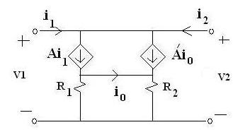
I want to design and simulate a good CCCS, but I am newbie, please give me some architecture and schematics
which stucture is good for this?
 

Technically, a current mirror is a CCCS. If you then add a cascode and or current mirror boosting it becomes more ideal. As for schematics, just google current mirror, cascode current mirror, or boosted cascode current mirror and you get all schematics.

Hope this helps,

JGK
 
Technically, a current mirror is a CCCS. If you then add a cascode and or current mirror boosting it becomes more ideal. As for schematics, just google current mirror, cascode current mirror, or boosted cascode current mirror and you get all schematics.

Hope this helps,

JGK
Thanks jgk2004
I want to replace the CCCS block at this circuit with good structure but I dont know how do this?

8081583600_1358190327.jpg


several related comments are in this post
https://www.edaboard.com/threads/274548/
 

One question, if the minus is ground, then we don't care about the current of the bottom line between R1 bottom and R2 bottom... But the top wire between the CCCS's, is this a mistake and should just be removed???....I think it should be removed since if it is there V1=V2... and therefore is kinda pointless.... If it is a mistake you can just put the current mirror in for Ai1 and A'i1 which each transistor in the place of each CCCS then make it do whatever input output you are looking for.

Hope this helps

JGK
 

There seems to be information missing. What is the purpose of this circuit? if you simplify this and say Ai1=x and Ai0 =y, temporarily ignore the relationship of i0 to Ai0, then you can say V0= (x+y)* (R1*R2)/(R1+R2), and IR2=V0/R2 and IR1=V0/R1, substituting gives you IR1=(x+y)*R2/(R1+r2), and IR2=(x+y)*R1/(R1+R2), so i0 = ((R1-R2)*(x+y))/(R1+R2) , now say y = i0 * A , this gives you => a loop because the equation for I0 contains itself. Someone please correct me if I am wrong.
 

Status
Not open for further replies.

Part and Inventory Search

Welcome to EDABoard.com

Sponsor

Back
Top