Continue to Site

Welcome to EDAboard.com

Welcome to our site! EDAboard.com is an international Electronics Discussion Forum focused on EDA software, circuits, schematics, books, theory, papers, asic, pld, 8051, DSP, Network, RF, Analog Design, PCB, Service Manuals... and a whole lot more! To participate you need to register. Registration is free. Click here to register now.

[SOLVED] CST Studio Microstrip Monopole Antenna Simulation

Status
Not open for further replies.

Radike

Member level 3
Joined
Aug 24, 2008
Messages
58
Helped
1
Reputation
2
Reaction score
1
Trophy points
1,286
Activity points
1,722
Hi All,

I am trying to simulate a Bluetooth Microstrip monopole antenna in CST studio. The design was taken from Nordic Semiconductor's nRF52840 dongle (https://www.nordicsemi.com/Software-and-tools/Development-Kits/nRF52840-Dongle) reference design.
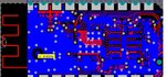
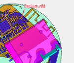
Please see below a image of the PCB. It does not have a ground plane underneath.

cst_antenna_1.jpg


Above image is taken from the reference design given by Nordic Semiconductors. I am now trying to simulate the above antenna in CST Microwave studio.
In the above image circuitry from the green arrow to the right is the matching circuit to the chip. I wanted to simulate the antenna to the left of the green arrow and then include the matching circuit first.
Substrate details are as follows (Actual fabricated dimensions):
FR-4 - Dielectric 4.8
h = 78.74 mil
Antenna microstrip trace width, w = 10 mil

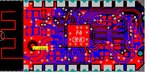
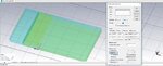
I have modeled the above circuitry (Antenna to the left of the green arrow) in CST Microwave studio. Please see the attached image below.

cst_antenna_2.jpg


cst_antenna_3.jpg


My questions are as follows:

1. How can I assign ports to a such a monopole antenna in CST?
2. Should I use a Waveguide port or a discrete port. In this case I don't have a ground.
3. I tried to use CST Maxros->Ports-> Calculate port extension coefficient and gets the following massage.

cst_antenna_4.jpg


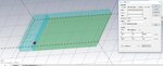
4. I manually created a waveguide port with the following dimensions:

waveguide width = 7*w
waveguide hight = 6*h
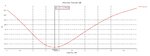
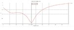
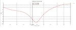
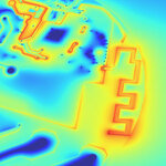
But the results were very bad. Please see the images below. Because of the w/h dimensions, port looks wired. But these are the actual widths and heights
they have used in the design.

Is it possible to know the correct way of simulating such an antenna?

cst_antenna_5.jpg


cst_antenna_6.jpg
 

The antenna is incomplete, a monopole can't work without a ground plane, in this case right of the feed point. The discrete port will be connected between the ground plane and the feed point.
 
  • Like
Reactions: Radike

    Radike

    Points: 2
    Helpful Answer Positive Rating
Hi FvM,
Many thanks for the reply.
Should I draw a separate ground plane to the right of the current feeding point?
Or the ground should be defined in the discrete port? I get the following box when I select the discrete port.
What X1,Y1,Z1 and X2,Y2,Z2?

cst_antenna_7.jpg
 

Hi,

In the nRF dongle, RF feeder line width is 35 mil which I think had calculated as a CPW. So I added a feeding CPW Microstrip line to the antenna with width 35 mil. Now I am getting some what sensible result, but the return loss is still not very good yet.

Below please see the images of the new port configuration and the results. Any idea what I am doing wrong. I am also getting some warnings while running the simulation.

cpw_discrete_port.jpg
cpw_discrete_port_S11.jpg
 

I have simulated and designed many of these PCB antennas for clients.

It is absolutely critical and important to include the true PCB ground size, which acts as an integral part of the antenna. Your model will not give useful results with the small pro-forma ground that you show. Model PCB ground in real size. The port type isn't critical, you can use a lumped port.

 
  • Like
Reactions: Radike

    Radike

    Points: 2
    Helpful Answer Positive Rating
Hi Volker,
Many thanks for the reply.
What I wanted is to do a simulation on just the antenna section and then add separate lumped element matching network so that I can match with the impedance of the nRF chip ANT port. Is it ok to add the entire ground plane and then add matching network separately?
I have attached an image of the actual top layer and bottom(Blue - Ground) layer PCB design.
As you can see, the blue color ground plane is not completely a plane. In this case should I draw a one big ground plane with the same size as the circuit?
I am also bit not clear on applying discrete port positive and negative port pin definitions. Based on the impedance calculation, the RF feeder width is calculate as considering it as a CPW. However, I do also get a ground plane underneath of this line. In this case should I also select this plane as a negative port pin as well?
Removing the bottom ground plane in my above simulation gave me a 9dB return loss. But this won't be same as the actual as there is a ground plane below .
 

Attachments

  • dongle_blue.jpg
    dongle_blue.jpg
    91.9 KB · Views: 156
  • dongle_red.jpg
    dongle_red.jpg
    113.5 KB · Views: 168

The question was about antenna simulation which needs 3D full wave solver. As volker explained, you should model the actual ground plane dimensions, I'd suggest as a rectangle.

Although the plane is has some voids, it's still mostly continuous. Outcome of the simulation is the antenna impedance at the feed point and optionally its radiation characteristic.

I assume that the coplanar line with ground doesn't significantly couple to the free field and can be simulated separately with more simple tools, if necessary at all.

Things are a bit more complicated if additional conducting planes and cables are connected to the ground plane and thus become part of the antenna.
 
  • Like
Reactions: Radike

    Radike

    Points: 2
    Helpful Answer Positive Rating
Hi FvM,
Thanks for the information. I tried simulating with the actual ground plane size. One with CPW feeder and another without CPW feeder.
Please see the images below.
Result were really bad when I did not include the CPW feeder.
With CPW its much better. I created a larger waveguide port with height about 5*h starting from the bottom ground plane and width 2*feeder width. Changing the waveguide port width to 3*feeder width shifted the curve to the right. I am not sure why this is so. Let me know your thoughts, suggestions on this.
Should I always include such a 50 Ohm feeder when I simulate Antennas?
In the actual PCB, there is 1.5pF capacitor just at the feeding point I am not sure how to include that. Any suggestion on how I can include this or what would you recommend?

Thanks a lot
 

Attachments

  • entire_ground.jpg
    entire_ground.jpg
    154 KB · Views: 207
  • entire_ground_S11.jpg
    entire_ground_S11.jpg
    170.5 KB · Views: 166
  • entire_ground_CPW.jpg
    entire_ground_CPW.jpg
    210 KB · Views: 160
  • entire_ground_CPW_S11.jpg
    entire_ground_CPW_S11.jpg
    148.3 KB · Views: 170
  • entire_ground_CPW_S11_Port_Width_3times.jpg
    entire_ground_CPW_S11_Port_Width_3times.jpg
    172.4 KB · Views: 183

    landho

    Points: 2
    Helpful Answer Positive Rating
What I wanted is to do a simulation on just the antenna section and then add separate lumped element matching network so that I can match with the impedance of the nRF chip ANT port. Is it ok to add the entire ground plane and then add matching network separately?

Yes, you can simulate the antenna with an (approximate) simplified PCB ground.
The port is then connected between the antenna feed and that ground. Indeed, matching can be done later using that 1-port S-parameter result from EM.

I have attached an image of the actual top layer and bottom(Blue - Ground) layer PCB design.
As you can see, the blue color ground plane is not completely a plane. In this case should I draw a one big ground plane with the same size as the circuit?

Yes, I think you can do that simplification and make it a large rectangle. Your PCB ground is reasonably solid near the antenna, that is the most critical part.

In the final verification, I usually simulate with full PCB layout detail, but that is not a must.

Your PCB seems to be a module. What I do in these cases: include the motherboard where the RF module is mounted onto. It does make a difference in some cases.

I am also bit not clear on applying discrete port positive and negative port pin definitions.

I don't know CST port handing details. In general, place one end of the lumped port on the antenna feed and connect the other end to nearest PCB ground.

Good luck!
 
  • Like
Reactions: Radike

    Radike

    Points: 2
    Helpful Answer Positive Rating
Hi All,
Many thanks for your support.

Thanks!
 

I believe the approach of arbitrarily modifying the feed line or matching components isn't very systematic. Instead you would measure the antenna impedance as is and design a matching circuit in the second step. That's particularly suggested if you don't a achieve a good matching with trial-and-error method.
 

Hi FvM,
Based on my above simulations above, If I don't have a feeder line then I see a very poor return loss. Seems antenna impedance at the input is not matched to 50ohms. However, adding a 50 ohms CPW feeder line helped me to get a good return loss. Is this expected or there is some issue in my simulation setup?
Length of the feeder I used was 250 mils, much smaller than a quarter wave length at 2.4 GHz.
 

As FvM mentioned, your configuration is not recommended. The "trick" that makes your CPW feed work is not CPW itself, it is the related ground structure that comes with the CPW feed. That ground is on a different layer than the other testcase, and possibly different size. That ground is what changes your matching.

You should really use a practical port feed scheme (e.g. lumped port) and go from there. Mixing antenna ground into the feed (by making feed ground part of the antenna) will drive you crazy later when implementing the actual layout.

It seems that the original antenna design includes a series element, most likely for matching. So if you don't have 50 Ohm for the antenna itself, that my be correct.

Good luck!
Volker

PS: Below I added what my simulation models look like, using a lumped port. Then, feed and ground for the antenna is modelled in a realistic way. You can simplify, but don't add in artificial elements like a large port that doesn't exist in hardware.
 

Attachments

  • model_detailed.jpg
    model_detailed.jpg
    230.2 KB · Views: 153
  • efield.jpg
    efield.jpg
    53.9 KB · Views: 174
Last edited:
  • Like
Reactions: Radike

    Radike

    Points: 2
    Helpful Answer Positive Rating
Hi Volker,

Thanks for the reply.
So the best approach is to model the actual circuit as closed as possible to the real PCB in CST and use a lumped port at the antenna feed point and then use this simulated data to add the matching circuit?

When you say lumped port, in CST this is equivalent to Discrete Port right?
Because there is no "Lumped Port" option in CST.
 

Yes, lumped port = discrete port.

Simplification: only as much as it doesn't change the ground situation (ground currents) seen by the antenna. It is a trade-off if you want fast simulation in the design phase. You might want to do some test cases in the beginning, then later you have experience how much simplification is "safe".
 
Last edited:
  • Like
Reactions: Radike

    Radike

    Points: 2
    Thanks, this helped a lot.
Thanks Volker,
Appreciate the support given. I will try out and see.
 

Status
Not open for further replies.

Part and Inventory Search

Welcome to EDABoard.com

Sponsor

Back
Top