Continue to Site

Welcome to EDAboard.com

Welcome to our site! EDAboard.com is an international Electronics Discussion Forum focused on EDA software, circuits, schematics, books, theory, papers, asic, pld, 8051, DSP, Network, RF, Analog Design, PCB, Service Manuals... and a whole lot more! To participate you need to register. Registration is free. Click here to register now.

<CST> Microstrip bend and wilkinson power splitter .

Status
Not open for further replies.

Pushhead

Full Member level 4
Joined
Jan 19, 2005
Messages
198
Helped
20
Reputation
40
Reaction score
10
Trophy points
1,298
Activity points
1,870
microstrip bend

Hello All,

Background story :

I'm designing a 2-way microstrip wilkinson power splitter in CST MWS. After a succesfull design of the basic splitter (S21~-3dB, S11<-20dB over most of the desired bandwidth) I have extended the output lines and added a 90 ° bend to both lines (design limitations).

The problem:

The 90 deg. bend have changed the S-parameters dramatically! i.e. S21,S11 have moved to a lower frequency.

Additional information:

The bend (line chamferring) was optimised for optimal S11 in a seperate model.
Boundary conditions are "Electric" with some added space above the lines.
Input port (50 Ohm) is at the bottom side of the PCB.
Output ports (50 Ohm) are at the Upper side of the PCB.

I know the splitter's response shouldn't change so drastically...
Can you help me with this ?

Tnx alot.
P.
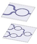
 

design the bends in microstrip

Can you provide a drawing of your layout so we can take a look? Together with the CST MWS design files?
 
  • Like
Reactions: edf

    Pushhead

    Points: 2
    Helpful Answer Positive Rating

    edf

    Points: 2
    Helpful Answer Positive Rating
microstrip wilkinson splitter

Here are the model script files (CST MWS 5).

I hope you can help me with this...

Tnx alot,
P.
 

bend microstrip in cst

I'd really appreciate it if someone could take a look at the design and give me his/hers opinion...

Tnx.
P.
 

Re: <CST> Microstrip bend and wilkinson power splitter

At 4.86 GHz, IS and RL seems to be >20 dB, IL is about 3 dB. What was the performance prior to adding the 90° bends?
 

    Pushhead

    Points: 2
    Helpful Answer Positive Rating
Re: <CST> Microstrip bend and wilkinson power splitter

The results showed the same but at 5 GHz ...
You see, the problem here is that adding bends changes the S11 pattern too much in my opinion.
I've optimized the bends separately, and got a "near-flat -40dB" response between 4 and 6 GHz. So introducing a bend to the splitter shouldn't change the VSWR significantly, not to mention changing the center frequency ...

What do you think ?

Tnx, P.
 
  • Like
Reactions: MariaC

    MariaC

    Points: 2
    Helpful Answer Positive Rating
Re: <CST> Microstrip bend and wilkinson power splitter

This happened for me too. When I vary the lengths of the output arms it changes operating frequencies.

The best thing to do is, draw the required structure and change the parameters of the wilkinson splitter to get the required performance and build it. Then it works fine. I've done this several times and they are working very well.
 

Hello Pushhead,

From your excellent description of the problem I see why you are concerned. I would not expect a large change with the addition of the bends either. (How large is large?) "Stripline Circuit Design", Harlan Howe, Jr. has a discussion of bends, pages 48-50, that I find useful. I note that you are using microstrip, not stripline, but the results are similar. Ansoft Designer has a canned miter tool (MSBENDO) with additional information. The documentation has a 138 exponent where it should be 1.38 so don't get confused by the typo. The results are similar to Howe. I would also be somewhat suspicious about a reported -40 dB S11. That is great, but probably not realizable. I would not get excited about a change from -40 dB to -20 dB for example.

I would be inclined to look at the model and see if something had gone wrong there as well. I would echo what Per_Lube suggested, iterate on the combined model to get back to your desired performance, then build the thing and test real hardware. The objective is functioning hardware not a computer simulation ..... unless, of course, you happen to sell software.

Regards,

Azulykit
 
hi
any body know how to design 8-way microstripline power spliter in CST. I need to feed 8 elements array antenna. i don't have any design parameter for the above power splitter. please help me to design this in CST as soon as possible.

Thank you
 

Hi kaandee,

The simplest way to design 8 way power splitter for an antenna is using 7 seven t-junctions. First with a t-junction divide into two. Then each output is divided into two with two more t-junctions. Then outputs of these t-junctions is divided with four more t-junctions. Finally you get 8 outputs. Output of each t-junction can be transformed back to the input port impedance with quarter wave length transformers.(t-junction output impedance become doubles at output ports ie. 50 ohm --> 100 ohm)

For narrow band antennas quarter wavelength transformers should be fine. If your antenna is a UWB one, you may need to use a different impedance transformation technique like tapered line.

There are many methods to design multiple output power splitters, but for feeding elements of an array those may not be suitable or design would be difficult due to the fact that keeping same phase at each output.

hope this will be useful to you

regards,
per_lube
 

Hello,

I have designed 4 way equal Wilkinson divider with CST Studio, but S21, S31, S41, S51 parameters are approx -8.5 dB @2.45 GHz. They need to be about - 6 dB.

Also, S32, S42, S52, S43, S53 are about -9 dB which is too high.

Resistors are modeled by using Lumped elements. Impedance of line is correct and checked by Impedance Calculator in CST. Quarter-wave transformers are designed like parts of circle.
I have no idea how to improve results, so please help if you have any solution.

Here is screenshot of divider:

ImageShack® - Online Photo and Video Hosting
 

Hi dux1,

I think your structure of the wilkinson is not the proper one...
According to the way you've drawn the wilkinson, it is difficult to connect the chip resistor.
If you change the length of the arms of the wilkinson according to your implementation either gap between two output ports get changed or you need to take the input port backward.

Please look at this one : wilkinson_power_divider.JPG(copied from https://www.wpi.edu/Pubs/ETD/Available/etd-011411-110214/unrestricted/Thesis_Final.pdf)

Build a similar one like this and change the widths of the arms (circular sections) and change the lengths of the circular sections until you get the required performance.
Usually, in many practical implementations, calculated values are giving slightly different performance. So you need to do slight tuneups to get the desired performance for the calculated values.

regards,
per_lube
 
Last edited:

Hi per_lube,

thanks for your advice, I hope it will be useful. Today I will design Wilkinson with circular sections and compare results.

Before I start with this, I'm not sure which value is correct for ε, because there is two values: ε_relative=4.32 for FR4, and ε_effective=3.28
for FR4 @2.45 GHz.

I need correct value, because λ=c/(f*sqrt(ε))

So, when I use 4.32, λ=5.89 cm and for 3.28 > λ=6.76 cm and this can lead to wrong results :idea:

Thanks once again :smile:
 

hi
I hope you reach to good results, dux1. I want just to advice you to be carefull when defining the waveguide ports in CST. I look to the attached picture, the ports look smaller than required. the port width should be 6 to 10 time the feed line width and the port height should be 5 times the substrate height. the wrong definition of the port may results wrong S11. to make sure that both the port and input line impedance are correct, normalize the impedance to 50 ohm. the results should not change.
 
Re: microstrip bend

Hello All,

Background story :

I'm designing a 2-way microstrip wilkinson power splitter in CST MWS. After a succesfull design of the basic splitter (S21~-3dB, S11<-20dB over most of the desired bandwidth) I have extended the output lines and added a 90 ° bend to both lines (design limitations).

The problem:

The 90 deg. bend have changed the S-parameters dramatically! i.e. S21,S11 have moved to a lower frequency.

Additional information:

The bend (line chamferring) was optimised for optimal S11 in a seperate model.
Boundary conditions are "Electric" with some added space above the lines.
Input port (50 Ohm) is at the bottom side of the PCB.
Output ports (50 Ohm) are at the Upper side of the PCB.

I know the splitter's response shouldn't change so drastically...
Can you help me with this ?

Tnx alot.
P.

I did this recently for some K-band hardware. If the bend causes your Wilkinson's performance to screw up, your quarterwave lines aren't optimal. Change the length and width of the 70.7 ohms lines to get the insertion loss to their absolute minimums. Once you reach that point, adding the bends will not screw up the performance. The problem stems from the bend inducing additional reflections which are not being cancelled inside the Wilkinson (which points out that the design is not yet at it's optimum). The 50 ohm lines on my design didn't change from their nominal design, but the quarterwave sections were a bit different from the ideal values due to coupling interactions on a "real" PCB.

For the 90 degree bend, use an optimal mitered bend (see **broken link removed**). The math has been done for it loooong ago. In most cases, a simple m=0.5 miter (take square corner, cut it in half to make a 45-45-90 triangle) will work. Be sure the gap from inside of the bend to closest point on the opposite edge is not too small. If it's too tight, you might get over-etching when you fabricate it and your miter will turn out smaller than you had intended ("acid well" effect).
 

Status
Not open for further replies.

Part and Inventory Search

Welcome to EDABoard.com

Sponsor

Back
Top