fatchan
Newbie level 4
Hi All,
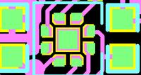
I noticed from my Gerbers that the solder paste (green), is not aligned with the copper footprint (pink) for my LLP package. I am using the standard package definition from Altium Protel for this package. I have never seen this before; usually copper and paste layers are aligned for component footprints.
Can someone help me take a look at the configuration and let me know if it will cause any issues during heat reflow?
Many thanks.
-Brian
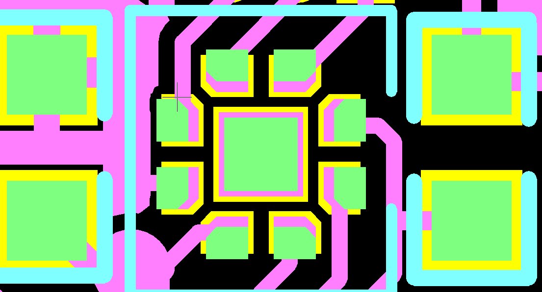