Continue to Site

Welcome to EDAboard.com

Welcome to our site! EDAboard.com is an international Electronics Discussion Forum focused on EDA software, circuits, schematics, books, theory, papers, asic, pld, 8051, DSP, Network, RF, Analog Design, PCB, Service Manuals... and a whole lot more! To participate you need to register. Registration is free. Click here to register now.

Connecting RF Tx/Rx Modules to SMA via PCB and header pin

Status
Not open for further replies.

jbpeckham

Newbie
Joined
Apr 14, 2021
Messages
5
Helped
0
Reputation
0
Reaction score
0
Trophy points
1
Activity points
65
Sorry if this looks similar to some other questions. I promise I've had a (quick) look around and can't find quite what I'm looking for.

Objective
I'm trying to design a remote control for a domestic system.

The prototype worked OK, using cheap and nasty 433 MHz OOK modules with straight 17.3cm monopole antennas. I'd like to build a version of the remote control which looks good enough to hold in the hand without a case. I'll design a good-looking PCB, epoxy it and make a sanded wood grip for the back of it.

But, that means I want something 'a bit more pro' than a bit of bent copper nicked from a power cable. Something like a quarter-wave monopole connected by an SMA. It doesn't have to go far - only a few metres and through a ceiling.

So, would this work?
  1. Design a PCB to hold the MCU, inputs, power, etc. etc.
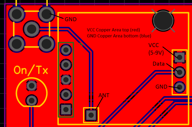
  2. Connect the 433 MHz OOK Transmitter parallel to and above the PCB via header pins
  3. Connect the Transmitter's ANT pad back down to the PCB by a header pin
  4. Trace the RF signal to the SMA, which is also connected to the Ground Plane
There's an image at the bottom (but I've already identified a few issues with it, see text above it).

RF Measures considered:
  • Transmission line on PCB < 10mm (wavelength of 433 MHz at ~0.5c would be approx. 350mm)
  • Impedance roughly matched to 50 Ohm: for 1oz copper under a solder mask and on the other side of a 1.4mm board from a ground plane, I figure ~100 mils trace width.
  • Transmission line on the opposite side of the PCB from the SMA connector (to minimise the effect of the through-hole stub)
  • Ground plane on the same side of the PCB from the SMA connector
  • I'll do my best to get a good solder joint
What have I missed?

Possible unknowns:
  • I understand the antenna ideally has a ground plane to reflect RF radiation off. That doesn't really exist here in any meaningful size. I guess that's OK though because the prototype worked?
  • Is the coiled stubby antenna going to be any less effective than the straight wire used before?
  • I've not considered any impedance matching of the header pin, and also assumed that any circuitry inside the off-the-shelf Tx module is irrelevant.
  • I don't know if mounting the Tx module parallel to the main PCB is better or worse than perpendicular.
  • I've seen some recommend a ground plane on both sides. Is that better, and would it change the impedance matching calculations?
  • It's just a monopole antenna and the ground connection back to the Tx module is distant from the antenna connection (next to the Data and VCC pins). Does that change anything?
  • My soldering is inconsistent :D
I've included a picture below which is not 100% what I'm describing. Since drafting the PCB below I plan to shorten the trace, to switch the top and bottom copper planes so the trace is on the bottom and the ground plane is on the top, and also remove the VCC plane in the vicinity.

dc0b7d2cbde7db51170a32609b5793da08d88701.png
 

Many comments can be added to your design.Few of them..
-Transmission Line does not seem have 50 Characteristic Impedance, it's very thin.Use absolutely double layer PCB ( wholly underneath should be GND )
-If you can, find 90 Degree SMA Connector that will make the Antenna perpendicular to the PCB.
-Reserve some parallel and series SMD component places for eventual Impedance Matching ( not compulsory)
-Your system is not too critical, it will work for few meters even-tough you attach a fork to antenna..;)
Hello BigBoss,

Thanks for getting back to me. After a bit of a crash course over the last few days I've refined the design - all very similar to what you say. But perhaps you could just have a look for my sanity!?

Basically, I changed out the cheapo modules for the STX/SRX 882 modules which should be slightly better - and don't come with pins already inserted in the wrong place :D. I'll use bog standard header pins to connect it back to the PCB.

I also made the transmission line very short. I couldn't make it quite 50 Ohm because it needs to fit between the GND pins but shorter and fatter should get us closer.

PCB is double layer. All the traces are now on the reverse side and an uninterrupted ground plane on the component side. I've tried to leave a margin in 2 orthogonal axes but the screw holes still needed to be there.

Plan for SMA remains one that points straight 'up', with a straight antenna. That means the antenna will be perpendicular to the PCB. Antenna is a short helical stub for 433 MHz.

Component Side
Component Side.PNG

Reverse Side
Reverse Side.PNG
 

Hi,

I´d place a ceramics cap each on input as well as output of voltage regulator. Short traces.

All the supply traces could be a bit wider.

For my tatste the XTAL and capacitors are abit far away from the AVR, especially when there is another HF source around.

I´d add a capacitor at the RESET line. This has two benfits: It makes the node immune against HF pickup and it causes a debuced signal with a minimum RESET_ACTIVE time.

Are theAVR internal pullups strong enough for the keyboard multiplexing.
How do you handle multiply key press?

But all in all not bad.

Klaus
 

The layout looks well
-Don't use Thermal Reliefs for SMA Connector,instead use direct connection.
-Widen the tracks, there are so many spaces.Use Teardrop for track at the end of Pads.( for long durability)
-Place VIAS to strengthen GND connection.
 

Hi,

I´d place a ceramics cap each on input as well as output of voltage regulator. Short traces.

All the supply traces could be a bit wider.

For my tatste the XTAL and capacitors are abit far away from the AVR, especially when there is another HF source around.

I´d add a capacitor at the RESET line. This has two benfits: It makes the node immune against HF pickup and it causes a debuced signal with a minimum RESET_ACTIVE time.

Are theAVR internal pullups strong enough for the keyboard multiplexing.
How do you handle multiply key press?

But all in all not bad.

Klaus
Hi Klaus, that's great feedback thanks, especially as I was only really asking about the RF elements! I've got an Aluminium cap on each side of the LM7805 regulator, which is as per it's recommended circuit, but admittedly I've positioned them a little further away than ideal. Same again for the XTAL - I prioritised placing the RF module and 100nF cap. I'll see what I can do. I'll also boost the supply traces a little.

The keypad worked fine in the prototype (4x4 keypad 1x8 header directly soldered into Arduino Micro). I've not dealt with multiple key presses yet and off the top of my head the result would be to preferentially select the uppermost and leftmost key.

Like I say, thanks for all your feedback - definitely going beyond the simple tutorials you see online!
 

The layout looks well
-Don't use Thermal Reliefs for SMA Connector,instead use direct connection.
-Widen the tracks, there are so many spaces.Use Teardrop for track at the end of Pads.( for long durability)
-Place VIAS to strengthen GND connection.
Mega, thanks BigBoss. I'm not sure I understand your first point - the SMA Connector is just 5 x plated through-hole pads.
 

Hi,
I've got an Aluminium cap on each side of the LM7805 regulator, which is as per it's recommended circuit,
interesting. TI datasheets tells:
*Although no output capacitor is needed for stability, it does help transient response. (If needed, use 0.1-μF, ceramic
disc).

Nothing about aluminum. Aluminium electrolyte is slow. And if a standard one, then may have high ESR.
When HF is nearby I always recommend to use fast enough capacitors. Just to "protect" the regulation loop to be confronted with this external HF.

I don´t say it does not work.. it´s just more safe. Adding the capacitors at the PCB layout won´t cost anything. Then you are free to assemble them or not.
But it maybe safes from a redesign.

Klaus
 

Hi,

interesting. TI datasheets tells:
*Although no output capacitor is needed for stability, it does help transient response. (If needed, use 0.1-μF, ceramic
disc).

Nothing about aluminum. Aluminium electrolyte is slow. And if a standard one, then may have high ESR.
When HF is nearby I always recommend to use fast enough capacitors. Just to "protect" the regulation loop to be confronted with this external HF.

I don´t say it does not work.. it´s just more safe. Adding the capacitors at the PCB layout won´t cost anything. Then you are free to assemble them or not.
But it maybe safes from a redesign.

Klaus
Good point, looking back most of the circuit diagrams do show ceramic (or at least, symmetric) caps. It just so happens that the ATMEGA328 'pack' I picked up off Amazon had aluminiums for the power circuit. I'll see what I can find cheaply. Perhaps it's time to pick up a mixed box of ceramics.

Thanks again Klaus!
 

Hi,

100n ceramics is the most used capacitor, at least at my designs.

An aluminum for a microcontroller makes no sense.

Klaus
 

Status
Not open for further replies.

Part and Inventory Search

Welcome to EDABoard.com

Sponsor

Back
Top