Continue to Site

Welcome to EDAboard.com

Welcome to our site! EDAboard.com is an international Electronics Discussion Forum focused on EDA software, circuits, schematics, books, theory, papers, asic, pld, 8051, DSP, Network, RF, Analog Design, PCB, Service Manuals... and a whole lot more! To participate you need to register. Registration is free. Click here to register now.

Complementary Self Biased Compartor Design

Status
Not open for further replies.

kah89

Junior Member level 2
Joined
Feb 9, 2015
Messages
24
Helped
0
Reputation
0
Reaction score
0
Trophy points
1
Activity points
169
Hi,

I am trying to design very low power self biased comparator like the one in the attached picture and I am loading the output with two inverters

I need to know what is the design procedures I have to follow also any materials would help a lot

Thank you.

SBC.PNG
 

Did you get this circuit from paper?

Here's another one with a nice description.
 

Did you get this circuit from paper?

Here's another one with a nice description.

I got it from Bazes paper , Thank you for the document but still I don't know how to determine the sizing of the transistors

I tried to design one it operates only when the input voltage is high
 
Last edited by a moderator:

Thank you for the document but still I don't know how to determine the sizing of the transistors

I tried to design one it operates only when the input voltage is high

Part 3 of the above linked document gives you optimization hints for the W/L ratios.

The necessary W/L ratios essentially depend on the process used, its p/n mobility ratio, and your priority either for speed, ICMR, or sensitivity.

For more help you should unveil this info, and the design schematic you've used so far.
 

    V

    Points: 2
    Helpful Answer Positive Rating
Part 3 of the above linked document gives you optimization hints for the W/L ratios.

The necessary W/L ratios essentially depend on the process used, its p/n mobility ratio, and your priority either for speed, ICMR, or sensitivity.

For more help you should unveil this info, and the design schematic you've used so far.


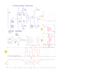
My priority is for power and speed I attached the same schematic I have used 111.png


Low power and speed are two opposing trends - you have to decide on a compromise.


Without mentioning your process, and without your W/L ratios, it doesn't make much sense.

Low Power is my first

The process is UMC 0.13 and I am using minimum sizing for all transistors (3.3 transistors, W/L=160n/340n)
I am still a beginner in design so I really appreciate your help
 

Low Power is my first

The process is UMC 0.13 and I am using minimum sizing for all transistors (3.3 transistors, W/L=160n/340n)

I don't have the UMC 0.13 models, so I tried with 0.18µm models. I think you could use the W/L ratios, perhaps scale them down a bit. But don't use min. size transistors (if you don't need max. speed).
2_comp_self_bias.png

Note:
I've used just one additional inverter, guess that's enough. In this case, the pos. and neg. inputs have to be swapped (relating to Vout1).

The ICMR is only about VDD/2 ± 250mV .

I think you could start from this schematic.
 
  • Like
Reactions: kah89

    kah89

    Points: 2
    Helpful Answer Positive Rating
I don't have the UMC 0.13 models, so I tried with 0.18µm models. I think you could use the W/L ratios, perhaps scale them down a bit. But don't use min. size transistors (if you don't need max. speed).
View attachment 116492

Note:
I've used just one additional inverter, guess that's enough. In this case, the pos. and neg. inputs have to be swapped (relating to Vout1).

The ICMR is only about VDD/2 ± 250mV .

I think you could start from this schematic.

Thank you very much it works now, but one last thing when I increase the supply it doesn't work properly. Thanks again
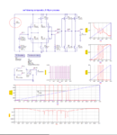
 

... when I increase the supply it doesn't work properly.

In this case decreasing the W/L ratios of M3 & M4 in proportion to the "inner" transistors may help:

3_self-bias_comp.png

Note:
  • I've scaled down the W/L ratios by a factor of 2 - these should be fine for your 0.13µm process, I hope.
  • Now a 2nd inverter stage is needed.
  • The ICMR is shown in the image.
  • As you know, I've used 0.18µm models. The circuit might not work with your models.
Good luck!
 
  • Like
Reactions: kah89

    kah89

    Points: 2
    Helpful Answer Positive Rating
In this case decreasing the W/L ratios of M3 & M4 in proportion to the "inner" transistors may help:

View attachment 116515

Note:
  • I've scaled down the W/L ratios by a factor of 2 - these should be fine for your 0.13µm process, I hope.
  • Now a 2nd inverter stage is needed.
  • The ICMR is shown in the image.
  • As you know, I've used 0.18µm models. The circuit might not work with your models.
Good luck!

Thank you very much I really appreciate your help
 

I have a problem with this comparator, as long as the input is lower than half of the supply it doesn't work properly?
 

Try to adjust the width ratio W(PMOS)/W(NMOS) to the low-field mobility ratio U0(NMOS)/U0(PMOS) of your process. It's probably close to 3 . You can find the U0 values in your models.
 

Try to adjust the width ratio W(PMOS)/W(NMOS) to the low-field mobility ratio U0(NMOS)/U0(PMOS) of your process. It's probably close to 3 . You can find the U0 values in your models.

I did but with the same problem, Why the input has to be greater than half of the supply?
 

Why the input has to be greater than half of the supply?

This depends on individual W/L ratios, and of those ratios between the transistors. Play with them! Try increasing M4 and/or decreasing M3. See if this works in the required direction, and iterate, if necessary.
 

Status
Not open for further replies.

Part and Inventory Search

Welcome to EDABoard.com

Sponsor

Back
Top