Continue to Site

Welcome to EDAboard.com

Welcome to our site! EDAboard.com is an international Electronics Discussion Forum focused on EDA software, circuits, schematics, books, theory, papers, asic, pld, 8051, DSP, Network, RF, Analog Design, PCB, Service Manuals... and a whole lot more! To participate you need to register. Registration is free. Click here to register now.

compensation of CMFB loop

Status
Not open for further replies.

jimito13

Advanced Member level 1
Joined
Nov 17, 2008
Messages
464
Helped
130
Reputation
262
Reaction score
113
Trophy points
1,323
Location
Greece
Activity points
4,929
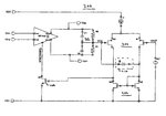
Hi,my CMFB loop consists of a two stage miller compenstated opamp with PM>60deg but when i add the circuit on my opamp i get negative phase shift (phase begins from 180deg at the stb analysis of cadence spectre and @ unity gain freq of the loop PM<0).How can i compensate my loop??I must note that i tried to put the 2 capacitors in parallel with the sensing resistors with no result...PM remains negative...

Thanks in advance for any helpful answer.
 

Typically the CMFB loop is single ended. I think you have too many loops in the system.
try single pole opamp for CMFB and decide and makes its output pole the dominant one. you should be ok
 

my cmfb loop is single-ended,as i said a single-ended two stage opamp in order to get the high gain that is needed as the simulations with ideal cmfb indicated me.I have three cmfb loops,one for the main OTA and two for the gain boosters.all are identical.any other suggestion on this kind of cmfb?
 

Sorry I didn't mean single ended. I meant single stage.
So use a single stage opamp and make the o/p pole the dominant one. ok
 

The problem could be often that the

CMD feedback transfer function of the external opamp connection

have a less favorable effect to the connected loop gain.

For better diagnosis a schematic is helpful. A strategy is to assign the CMD control less gain within the opamp. If the CMD regime is medium output voltage sense and control similar current summing junctions via gm-diff-amps you get similar gain than the differential mode.
 

rfsystem thanks for your answer but could you please be more clear?i didn't quite understand what you said...i will upload a schematic later.thanks.
 

I have the same question that love_analog had. Why are you using a two stage opamp for the CMFB?? I think you're adding more gain that what you need and at the same time loosing phase margin without need for it. Remember that when you add your CMFB to your circuit you have additional poles in the system which degrades the overall PM

diemilio
 
i use two stage CMFB because my simulations with ideal cmfb indicated me high gain for the cmfb circuit (as an independent entity) that cannot be achieved with only one stage.

why cmfb will degrade the overall phase margin??it is just a dc circuit that will not affect the ac signal since it doesn't pass from inside it...pole zero analysis confirms my claim since no additional poles and zeros come up on the plot.
 

Most of the gain in the CMFB loop is usually given in the main amplifier itself and not by the CMFB amp (this amp has usually relatively low gain), but all this depends on your architecture. You need to upload your schematic

diemilio
 

My opamp is a folded cascode opamp with gain boosting technique applied.The circuit is quite large so i avoid to upload it for simplicity,but everybody understands my topology i suppose.

Below i show you my cmfb circuit.

After the opamp outputs and before the sensing resistors i use ideal voltage buffers that are not shown on the pic.(does somebody have any idea how to implement these buffers with real circuits in a way different from common drain so as to avoid dc shift?)

Also i do not show the compensation caps in parallel with sensing resistors since the didn't work for me.
 

Are the capacitors straightly in parallel with the resistors? If so, these are NOT compensations caps, these are used to speed up the CFMB response!!! Your CFMB dominant pole is usually determined by the load capacitance of the whole circuit. What you usually do to compensate is increase this capacitance at the expense of deteriorating the BW of the main amplifier. If the trade off is not good enough then you usually lower the gain of the CMFB loop.

It seems to me that you are a little bit confused with your circuit implementation, you should probably go through all the equations and make sure you fully understand where each pole of the system is located and what are the implications of changing their values.

diemilio
 

Yes they are straightly in parallel with the sensisg resistors.Everywhere i read that these caps compensate the cmfb,nobody says about speed up...How would you set them in order to compensate instead of straight parallel connection??

I cannot increase my load capacitance since GBW limitation is not desired for me.Can you propose me any good reference to go about all those equations of cmfb you mentioned?

Added after 2 hours 11 minutes:

I try what you suggested above.I left for common mode feedback only the first stage of the picture uploaded (without the 2nd stage-common source).It seems to work better and connecting a capacitor properly along with the two other capacitors it seems to be compensated.

One more question : Is it significant in which side of the diff pair of the cmfb i will connect the common node of the sensing resistors?
 

does anybody have any idea how to achieve the compensation/pole splitting procedure for the one stage cmfb (diff pair with current mirror load) ? i put a compensation capacitor from the common node of the sensing resistors to the diode connection of the current mirror but i cannot achieve PM>45-50deg.....

diemilio since you proposed me to look through the equations of cmfb yesterday,how would you try to compensate a one stage (as mine) continuous time cmfb?
 

Yes, it is important where you connect the common node of the sensing resistors; you must guarantee that the overall CMFB is stable (180 deg) so if you switch the inputs of the CFMB amp you will pass from a non-inverting to an inverting configuration (or vice-versa) and this will make the loop unstable.

For that particular configuration you can only reduce the gain of the CMFB loop or increase the output pole of the amplifier to get better PM because that's where your dominant pole is located.

Chapter 12 of Gray, Hurst, Lewis & Meyer (and especially section 12.4) has a very very good explanation on Fully Diff amps and on how to include and compensate the CMFB. The shown techniques are very basic though, so if you need something a little bit more sophisticated (but no too complicated) check chapter 26 of Baker, there he as a Switched Capacitor CMFB scheme which is very helpful if your overall design is a switchcap camp or filter. You can also check section 9.6 of Razavi; he has very similar concepts as the ones shown in Gray...Meyer but with more examples and less theory.

diemilio
 

As far as the common mode node i agree with you since the feedback should be negative,i realized that a few moments after posting the question here!So changing the polarity of the feedback amplifier inputs the type of feedback changes and the loop become unstable and does not work as expected.

I have already gone through all the references you mentioned...My application is not SC so i avoided the choise of a SC CMFB loop...

As i wrote in a previous post,i left just the one stage (diff pair with current mirror load) of the feedback amp to check the stability.The loop gain still remains satisfactory but PM hardly reaches 50deg and this is achieved only if i insert a capacitor like in the pic i will show you below.

The dominant pole at the output of the amplifier is created from the pair of the sensing resistors and the capacitances in parallel,right?I tried to tweak their values and find an optimum pair for their values but i didn't have any good result.

Also,the last and most importang thing is that : Although i get a PM at least 45deg as i said above i notice a strange overshoot at the loop phase plot as well as an "undershoot" (if i can use this term!) at the phase plot of the overall amplifier.

Regards
 

Attachments

  • 6774722-0-large_3903.jpg
    6774722-0-large_3903.jpg
    400.8 KB · Views: 136

Finally...one stage cmfb amplifier is not sufficient for my design as PVT corners indicated.With 2 stage cmfb amplifier things are ok but i cannot still compensate it...i would appreciate if somebody experienced to this design issue could give me some helpful advice.

Thanks in advance.
 

Why you connect your CMFB amplifier mirror load? is your gain then too much?

I would use 2 diode connected load, then your gm of CM input pair is mirrored into DM amp.

Personally think, if you want to use 2 stages as you showed, don't you need a Miller cap at second stage to compensate?

And what is C0 used for BTW?
 

Status
Not open for further replies.

Part and Inventory Search

Welcome to EDABoard.com

Sponsor

Back
Top