Continue to Site

Welcome to EDAboard.com

Welcome to our site! EDAboard.com is an international Electronics Discussion Forum focused on EDA software, circuits, schematics, books, theory, papers, asic, pld, 8051, DSP, Network, RF, Analog Design, PCB, Service Manuals... and a whole lot more! To participate you need to register. Registration is free. Click here to register now.

Comparing Capacitance multiplier with Zener diode series voltage regulator.

Status
Not open for further replies.

himanshul

Newbie level 5
Joined
Jun 21, 2011
Messages
9
Helped
0
Reputation
0
Reaction score
0
Trophy points
1,281
Activity points
1,395
Hi friends,

According to text…due to zener diode, Q1 is supplied with constant base voltage.
Any change in output voltage is sensed at at the emitter of Q1 which brings change in forward bias of the transistor. Thus transistor changes its resistance at CE junction and compensates for the voltage change at output or input.
Here transistor is acting as a variable resistor. Also total current pass through transistor hence it is also called as PASS transistor.

Q1.What all difference would it make, if I replace this zener diode with a capacitor and how would this circuit behave with a 1 Vp-p ripple is superimposed on 5V DC input signal??

I am having multiple queries regarding capacitance multiplier, will take them successively.

Source article- https://www.tpub.com/neets/book7/27k.htm
refer fig 4.34, 4.35, 4.36.
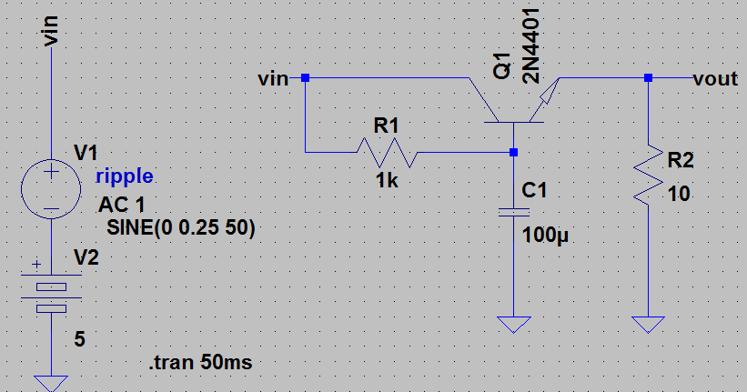
cap multiplier.PNG


Thanks!
 
Last edited:

Hi,

It sounds like homework.

I ask myself: The schematic is from a simulation software.
Why don't you just run the simulation an see what happens?

You could show the output voltage ... as well as any other current and voltage on a virtual scope.

Do this first, find out what exactly worries you, ask a specific question and upload the scope pictures you refer to, so we can discuss about it.

Klaus
 

The question text doesn't fit the schematic. There's no zener. Voltage regulator with zener and capacitance multplier have different purposes but also similarities. The latter is filtering ripple but not stabilizing the voltage to an absolute level. Both principles can be combined by connecting a zener in parallel to the capacitor.

Please clarify what you want to achieve.
 
With zener no longer present base is free to rise with input V, therefore emitter
also will rise, and you no longer have any V regulation.


The Zener presents a very low Z to base variation, and since base is ~ 1 Vbe above emitter, the Vout =
Vbe + Vz.

A sim might indicate otherwise but since Zener response to AC is very fast a C in parallel to it probably not
much different result.

Here 100 uF and then 1 pF, two runs, dashed line 1 pF, very little difference, because Vz is such low Z itself.
As you can see very small variation in load V with 2V pk-pk ripple at input to NPN.

1618678304591.png


Essentially you are placing a component in parallel with a V source, the Zener, and the V source dominates the response.

Regards, Dana.
 
Last edited:
Hi,

It sounds like homework.

I ask myself: The schematic is from a simulation software.
Why don't you just run the simulation an see what happens?

You could show the output voltage ... as well as any other current and voltage on a virtual scope.

Do this first, find out what exactly worries you, ask a specific question and upload the scope pictures you refer to, so we can discuss about it.

Klaus
Thanks for your reply,
I am looking it another way, first I am seeking to gain an intuition about how this circuit works, then I would be doing some circuit analysis to find out the values of circuit parameters and finally the last and the most important, i.e to run this circuit simulation to validate the results which I got from earlier phases.

However as you suggested I will certainly simulate this circuit to check what it says.
 

Hi,

You are free to do so. No problem.
This is how many electronics designer do it.

But from the question above it seems you are in the learning phase.
And for this you may play around with the simulation tool.
Run a simulation ... change the circuit ...run again simulation to see what happens.
Or change a part value....

Running a simulation costs nothing,
There will be no smoke, no explosion, no fire... and you don't need a huge stock of different part values.
And you get much faster feedback than with writing a forum post.

Klaus
 
Last edited:
With zener no longer present base is free to rise with input V, therefore emitter
also will rise, and you no longer have any V regulation.
Thanks for your reply.

Ok I got it what you are trying to point out.
With the presence of Zener the base voltage is held constant against any variation of source and load voltages and current, thus the output voltage is only the function of Vbe, as if Vout changes due to load variation consequently Vbe changes bringing about a change in resistance of the transistor at CE junction to compensate the change in output voltage.

But with the presence of capacitor
as, Vc = Vin - Ib.R1
and Vout = Vc + ~0.6
voltage at capacitor is dependent on Vin and since Vout is dependent on Vc, which means now Vout is now directly dependent Vin.
It can be concluded as now Vout is not immune to Vin fluctuation hence it changes accordingly with the source voltage.
Please clarify what you want to achieve.
Thanks for your reply.
Some couple of queries.

1.What is the exact role of BJT as an emitter follower in CM circuit??
-I assume that major amount of load current along with ripples pass through the pass transistor and then to load.
A discharge current from the capacitor also passes across the BE junction to load.
This means that there are 2 load currents which passes through the load resistor, one due to the pass transistor with major ripples and second is the discharge current of the capacitor.
If BJT will pass all the ripple to load then where and how ripples are minimised by this capacitance multiplier??

2.How capacitance multiplier makes the capacitance to "appear" larger. The effective value of cap with CM is CXβ, how to derive this expression??

-According to texts in order to make cap appears larger, the CM circuit reduces the load current. Since load current depends upon load value. If load changes it will change the cap discharge current. This discharge current will increase if the load value is small (i.e high load), hence making the capacitance to appears rather "smaller". If this is the case then where the statement that CM circuit multiplies capacitance hold true??
--- Updated ---

Hi,

You are free to do so. No problem.
This is how many electronics designer do it.

But from the question above it seems you are in the learning phase.
And for this you may play around with the simulation tool.
Run a simulation ... change the circuit ...run again simulation to see what happens.
Or change a part value....

Running a simulation costs nothing,
There will be no smoke, no explosion, no fire... and you don't need a huge stock of different part values.
And you get much faster feedback than with writing a forum post.

Klaus
Sure, I will love to do so.
 

But with the presence of capacitor
as, Vc = Vin - Ib.R1
and Vout = Vc + ~0.6
voltage at capacitor is dependent on Vin and since Vout is dependent on Vc, which means now Vout is now directly dependent Vin.
It can be concluded as now Vout is not immune to Vin fluctuation hence it changes accordingly with the source voltage.

But as you see from sim the Zener, due to low impedance, is constraining the voltage at the base of NPN to Vz.
Look at pk-pk at collector versus pk-pk out, or for that matter pk-pk V base of NPN.


Regards, Dana.
 
2.How capacitance multiplier makes the capacitance to "appear" larger. The effective value of cap with CM is CXβ, how to derive this expression??
-According to texts in order to make cap appears larger, the CM circuit reduces the load current. Since load current depends upon load value. If load changes it will change the cap discharge current. This discharge current will increase if the load value is small (i.e high load), hence making the capacitance to appears rather "smaller". If this is the case then where the statement that CM circuit multiplies capacitance hold true??
--- Updated ---


Sure, I will love to do so.
Typical and most important circuit for capacitance multiplication: MILLER integrator exploiting the MILLER effect.
 
Status
Not open for further replies.

Similar threads

Part and Inventory Search

Welcome to EDABoard.com

Sponsor

Back
Top