Continue to Site

Welcome to EDAboard.com

Welcome to our site! EDAboard.com is an international Electronics Discussion Forum focused on EDA software, circuits, schematics, books, theory, papers, asic, pld, 8051, DSP, Network, RF, Analog Design, PCB, Service Manuals... and a whole lot more! To participate you need to register. Registration is free. Click here to register now.

Comparator offset calculation

Status
Not open for further replies.

NadaElfamy

Newbie
Joined
Jun 2, 2021
Messages
1
Helped
0
Reputation
0
Reaction score
0
Trophy points
1
Activity points
18
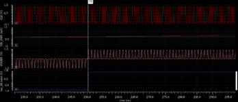
I have two questions, now i'am designing a comparator followed by Buffer then SR latch for ADC, and i wanna test the offset of this comparator, so i put a PWL (ramp input) in one of the inputs and a DC volt (VREF) in the other input,
First question: Should i check the output of the comparator or output from the SR latch (as the output of the comparator will suffer from the delay of the buffer and SR latch, so if i checked the output of SR latch this delay will be considered an extra offset).
Second question: And if it is not a difference, how should i calculate the offset from each one (comparator output or SR latch output).
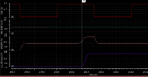
Comment: the second figure (capture2) is to clarify the delay of the comparator output and the SR latch output
 

Attachments

  • Capture.PNG
    Capture.PNG
    39.6 KB · Views: 165
  • Capture2.PNG
    Capture2.PNG
    28.2 KB · Views: 180

You will get an extra offset from the time delay since you sweep the input voltage continuously.

Since you use Virtuoso I would suggest building a binary search DAC in for example Verilog-A.
Flow:
1. Set initial differential voltage, vDiff, to 1 V
2. Output OutP = vCM+vDiff/2 and OutN = vCM - vDiff/2
3. On clock edge (after the SR latch has settled and then some) look at the output
3.1. If the comparator is high divide the vDiff with 2
3.2 If the comparator is low divide the vDiff with 2 and invert the polarity
4. Run for 16 clock periods to get 16 bits resolution.
5. Enjoy your problem-free and super-fast offset simulations with predictable runtime.

The above flow might contain some errors but you get the idea.
 
There is an error term in the transient ramp offset
voltage measurement scheme. It involves the ramp
dV/dt and the low-overdrive propagation delay
(which itself depends on input dV/dt, the slower
you go, the lower the overdrive and the longer
the delay). Your "measured" Vio will include ramp
dV/dt*Tpd error term.

Closed loop (ATE-style) testbenches take a long
time to run and this scheme also embeds some
error, from TPHL-TPLH asymmetry as the loop works
on the integrated (averaged) digital output voltage
and switching imbalance bends that. Not as badly
as with the ramp, if you designed the part with
decent delay matching.

Of course the ramp approach will be no good in
real test environments where noise probably
exceeds offset voltage, unless you way oversample
and take statistical median as your measurement.
 
Status
Not open for further replies.

Part and Inventory Search

Welcome to EDABoard.com

Sponsor

Back
Top