pcbman
Member level 5
Image in Design
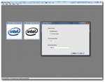
Image in Design changes each pixel of an image in drawing elements to PADS format. You can add and sign all printed circuit board with your company logo or all any symbols. Image in Design can change the dimensions of the image, improves its quality with Sharpen and Edges filters then finally transforms any colored image in black and white to be translated in Gerber format.


**broken link removed**
Image in Design changes each pixel of an image in drawing elements to PADS format. You can add and sign all printed circuit board with your company logo or all any symbols. Image in Design can change the dimensions of the image, improves its quality with Sharpen and Edges filters then finally transforms any colored image in black and white to be translated in Gerber format.


**broken link removed**
