Continue to Site

Welcome to EDAboard.com

Welcome to our site! EDAboard.com is an international Electronics Discussion Forum focused on EDA software, circuits, schematics, books, theory, papers, asic, pld, 8051, DSP, Network, RF, Analog Design, PCB, Service Manuals... and a whole lot more! To participate you need to register. Registration is free. Click here to register now.

Common Transistor Amplifier:- doubts on Input impedance

Status
Not open for further replies.

Qube

Member level 5
Joined
Nov 10, 2010
Messages
80
Helped
7
Reputation
14
Reaction score
7
Trophy points
1,288
Activity points
1,896
Hello friends,i had some doubt in designing a common emitter amplifier

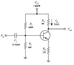
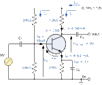
Here is the example schematic:-
**broken link removed**

1)Can you tell me its Input impedance value and the output impedance of that circuit

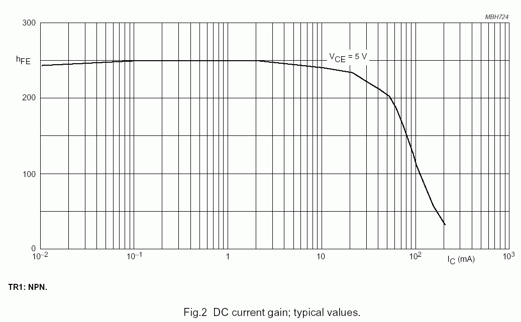
2)And as far as my knowledge,those coupling capacitors are used to pass AC in and out,and block DC to pass to next stage, and the capacitors can be used as filters..using
Cin=1/(2*pi x F x Zin)

Cout=1/(2*pi x F x Zout)

F is maximum frequency that the filter can let pass,any input frequency higher that F value will be rejected..
Am i right??

Please correct me if i'm wrong...would like to learn
 

Attachments

  • amp31.gif
    amp31.gif
    10.7 KB · Views: 88
Last edited:

Dear Qube
Hi
If the RE is double section ( one of them is bypassed and another not ) the Ri = R1 []R2 [] beta(re+RE) and rout = RC and about input and out put capacitors : those are pi filters ( between ri of this stage and rout of next stage ) but if you select that capacitor in reasonable value it will be short circuit .
however i don't know why i can't see your schematic ( can you attach it as PDF or as picture ?)
Best Wishes
Goldsmith
 

thanks for your reply gold smith,i have attached the image as attachment in the first post

And i didn't get this formula
Ri = R1 []R2 [] beta(re+RE)
is it
Ri=R1*R2*Hfe*(re+RE??)
 

No ! My mean was in parallel . ([] means in parallel !)
And re=Vt/Ic or IE and vt is thermal coefficient and will given by 11600/Temp ( at kelvin ) and for 27 degree (room degree ) it will be about 26 mv
And you bypassed all of your emitter resistor , thus you'll have Ri=R1 in parallel R2 in parallel beta*(re).
Good luck
Goldsmith
 

Oh,didn't know that symbol :)

Can you show me how you calculate the Input impedance of the circuit in this schematic??
amp31.gif
 

No ! My mean was in parallel . ([] means in parallel !)
And re=Vt/Ic or IE and vt is thermal coefficient and will given by 11600/Temp ( at kelvin ) and for 27 degree (room degree ) it will be about 26 mv
And you bypassed all of your emitter resistor , thus you'll have Ri=R1 in parallel R2 in parallel beta*(re).
Good luck
Goldsmith

Sorry, Goldsmith - it isn`t correct.

Input resistance:
Zin=R1||R2||h11 with h11=small signal input resistance of the BJT in CE configuration.
(This formula assumes that the emitter resistor Re is bypassed by Ce for all frequencies of interest)

Output resistance:

Zout=Rc||(1/h22) with Rc=collector resistor and h22=output conductance of the BJT (normally, can be neglected against Rc).

________________

Qube, your formulas for the edge frequencies are OK - again under the assumption that Ce sufficiently bypasses Re for the operating frequency.
 

Sure . but before that , the collector current calculated wrongly ! (12*3.6)/(3.6+20)=1.8(approx) 1.8-0.6= 1.2
1.2/220 =5.59 ==5.6ma(approx) ====> re = 26/5.6 =4.64 ohms.
R1 in parallel with R2 = (20*3.6)/(20+3.6) =====> Req =3k ohms ( approx) . and about beta . you can't say that beta is about 100 simply , because the specifications of each transistor is different from another type and the beta , depends on the quiescent point ( ib will given from curve tracer or datasheet ) ( you have vce and IC and thus according to the out put curve you'll be able to find ib and after that beta simply )
Anywhere , if we suppose that beta is about 100 thus we will have :3000 in parallel with 100*4.64 ====> 1146 ohms
Best Wishes
Goldsmith

---------- Post added at 19:30 ---------- Previous post was at 19:27 ----------

Dear LvW
Hi
Yes , but i told them with some usual approximations .
Yes i agree with this : zout = RC in parallel with ro and ro is 1/hoe and hoe is Va/IC and Va is early voltage . but i dont think at this quiescent point these parameters have sensitive effect , isn't it ?
Best Regards
Goldsmith
 

Sorry, Goldsmith - it isn`t correct.

Input resistance:
Zin=R1||R2||h11 with h11=small signal input resistance of the BJT in CE configuration.
(This formula assumes that the emitter resistor Re is bypassed by Ce for all frequencies of interest)

Output resistance:

Zout=Rc||(1/h22) with Rc=collector resistor and h22=output conductance of the BJT (normally, can be neglected against Rc).

________________

Qube, your formulas for the edge frequencies are OK - again under the assumption that Ce sufficiently bypasses Re for the operating frequency.

About the Formulas

Cin=1/(2*pi x F x Zin)

The capacitor will attenuate signals frequencies higher than the F value??

For example ,the F value is 100Hz..
so the Cin capacitor will attenuate(reduces the amplitude) input signal whose frequency is higher than 100Hz....Am i right???
 

Yes , but i told them with some usual approximations . .......

Goldsmith - your main error was the part
beta(re+RE) .

The input resistance at the base node of a BJT with Re-feedback is (re + h21*RE) (in your terms: re + beta*RE).

---------- Post added at 16:43 ---------- Previous post was at 16:38 ----------

_____________________________
The capacitor will attenuate signals frequencies higher than the F value??
For example ,the F value is 100Hz..
so the Cin capacitor will attenuate(reduces the amplitude) input signal whose frequency is higher than 100Hz....Am i right???


Qube, the input coupling capacitor - together with the amplifier input resistance - forms a C-R highpass.
That means that for frequencies well below the corner frequency the signal will be attenuated.
Well above this frequency the signal is passsed to the transistor input (nearly) without any loss.
 

Dear LvW
Again Hi
Yes , you're quite right .
Thanks for your remark.
Best Regards
Goldsmith

---------- Post added at 20:24 ---------- Previous post was at 20:20 ----------

But why when i measured the impedance of a CE amp with this formula the practical result and theoretic result was the same together ? it is thing that i think , at these Q points , i don't think this precision needed . can you compare the result of that formula with practical result , please ?
Again Thanks
 

Goldsmith - your main error was the part
beta(re+RE) .

The input resistance at the base node of a BJT with Re-feedback is (re + h21*RE) (in your terms: re + beta*RE).

---------- Post added at 16:43 ---------- Previous post was at 16:38 ----------

_____________________________
The capacitor will attenuate signals frequencies higher than the F value??
For example ,the F value is 100Hz..
so the Cin capacitor will attenuate(reduces the amplitude) input signal whose frequency is higher than 100Hz....Am i right???


Qube, the input coupling capacitor - together with the amplifier input resistance - forms a C-R highpass.
That means that for frequencies well below the corner frequency the signal will be attenuated.
Well above this frequency the signal is passsed to the transistor input (nearly) without any loss.

Yes,the Cin and input impedance of transistor circuit forms High pass filter...

you said " for frequencies well below the corner frequency the signal will be attenuated."

Its just my simple doubt that in the formula Cin=1/(2*pi x F x Zin) ,the F is the value of the frequency,my doubt will the CR filter attenuate signal above the F value or below the F value in the formula Cin=1/(2*pi x F x Zin)

---------- Post added at 17:00 ---------- Previous post was at 16:55 ----------

And i read in a book about calculating the input impedance

it says
1/Rin=1/R1+1/R2+1/Rin(base),ac

Rin(base),ac=hfe(Re*Rload/Re+Rload)

so regarding that schematic

Rin(base),ac=18.5K

1/Rin=1/20K+1/3.6K+1/18.5K
 

Its just my simple doubt that in the formula Cin=1/(2*pi x F x Zin) ,the F is the value of the frequency,my doubt will the CR filter attenuate signal above the F value or below the F value in the formula Cin=1/(2*pi x F x Zin)

Qube, do you know the difference between lowpass and highpass?
Think about the meaning of the term "high paass".

And i read in a book about calculating the input impedance
it says
1/Rin=1/R1+1/R2+1/Rin(base),ac
Rin(base),ac=hfe(Re*Rload/Re+Rload)
so regarding that schematic
Rin(base),ac=18.5
1/Rin=1/20K+1/3.6K+1/18.5K

The given expression for Rin(base) is not correct.
Apparently it applies to the emittter follower (common collector) because of Re||Rload.
More than that it neglects the term h11 - which may be allowed in case of the emitter follower only!
But in your case, Re is bypassed by Ce. Thus, don`t apply the wrong formula.
 
  • Like
Reactions: Qube

    Qube

    Points: 2
    Helpful Answer Positive Rating
Qube, do you know the difference between lowpass and highpass?
Think about the meaning of the term "high paass".
Sorry,high pass filter passes frequencies higher than the F value in Cin=1/(2*pi x F x Zin)... it attenuates frequencies lower than F...

---------- Post added at 19:23 ---------- Previous post was at 19:02 ----------

Qube, do you know the difference between lowpass and highpass?
Think about the meaning of the term "high paass".


The given expression for Rin(base) is not correct.
Apparently it applies to the emittter follower (common collector) because of Re||Rload.
More than that it neglects the term h11 - which may be allowed in case of the emitter follower only!
But in your case, Re is bypassed by Ce. Thus, don`t apply the wrong formula.

Thanks you for pointing out my mistake :)
and wat do you mean by h11 =hfe?
 

Qube,

The best way to find the input and output impedance is to use the General Immittance Theorem. This theorem states that the input impedance can be obtained from the denominator of the transfer function by setting solving for -Zs. Similiarly, the output impedance can be obtained by solving for -ZL. Don't forget that the source impedance affects the output impedance and the load impedance affects input impedance. Since you did not specify finite values for beta, C1, C2, and CE, the transfer equation will contain a lot of terms. After finding the input and output impedances, I simplified them by removing the capacitors and setting the load impedance to infinity and the source impedance to zero.

Ratch
 

Attachments

  • QUBE.pdf
    179.5 KB · Views: 70
  • QUBE_A.pdf
    1.3 MB · Views: 69
Last edited:

I'll put it more clearly friends,so that you can see if my knowledge is correct and i'm not confused..

i have attached the example schematic..

In that schematic,the
Vcc=12V
Iq=1mA
Hfe=100

Step 1:
i have chosen 1/2 Vcc at Vc to get full swing,so its 6V @Vc
so the resistor value of Rc = 6/0.001=6K

Step 2:

I have set the Ve to 1V for temperature stability
so Re = 1/0.001ma = 1K

Step 3:

Setting the value of R1 and R2 so that Vb = Ve+0.6V
so Vb should be 1.6V

finding the Ib
Ib=Ic/Hfe;
Ib=0.001/100= 0.00001

I will chose the value of R2 so that it drops 1.6V with providing current 10 times more than Ib so that the base voltage will be steady..

so 10*Ib=0.0001

R2= 1.6/0.0001 = 16K

so now R2 has dropped 1.6V ,now R1 has to drop 12-1.2 =10.8V
and has to provide 10+1 times the current for both R2 and the base

So R1 should provide 10*Ib+Ib
so its 0.0001 +0.00001 =0.00011 i.e 0.11mA

R1=10.8/0.00011 = 98K


so R1= 100K ,R2 =16K Rc=6K Re=1K

Step 4:- finding the Input impedance of the transistor..

here Rin is the combined parallel resistance of the voltage divider resistors, and Rin(base),ac

Rin(base),ac =~Hfe(rtr) rtr= transresistance

rtr =0.026 V/IC = 0.026 V/1 mA = 26ohms

rtr=26 Ohms
so the Rin = 1/R1+1/R2+1/100(26)
Solving this equation gives me ,Rin = 2.188K ohms (2.2K rounded figure)


Step 5:- calculating the Cin
Cin and the Rin forms the HPF,so if i need the filter to pass signals over 100Hz then F=100

Cin=1/(2*pi x F x Zin)

=1/(2*pi*100hz*2200)
Cin=0.723uF


So the Zin is 2.2Kohms resistance...

do you think my steps and calculations are right?? If i'm wrong plz correct me


Now i want to find out it output impedance...
 

Attachments

  • a2.jpg
    a2.jpg
    21.2 KB · Views: 61
Last edited:

Qube,

The best way to find the input and output impedance is to use the General Immittance Theorem. This theorem states that the input impedance can be obtained from the denominator of the transfer function by setting solving for -Zs. Similiarly, the output impedance can be obtained by solving for -ZL. Don't forget that the source impedance affects the output impedance and the load impedance affects input impedance. Since you did not specify finite values for beta, C1, C2, and CE, the transfer equation will contain a lot of terms. After finding the input and output impedances, I simplified them by removing the capacitors and setting the load impedance to infinity and the source impedance to zero.
Ratch

Hi Ratch,
question: Did you create the (funny) document Qube_A.pdf ? Do you expect somebody will read it?

Concerning your suggestion:
1.) Do you really believe that the "best way" to find input/output impedances of a BJT amplifier is to use the corresponding transfer function? What is the advantage if compared with the direct and classical methods?
2.) From the engineering point of you I disagree with "don`t forget that the source impedance affects the output impedance.....". I think this influence which is caused by the parameter h12 (backward gain) can and should be neglected because it influences the result certainly by less than 1% only. The same applies to the influence the load impedance has on the input impedance.
You shouldn't forget that in the area of electronics no formula is correct by 100% - and it is good engineering practice to introduce simplifications and to neglect some effects that are well below the limits of other unavoidable uncertainties (tolerances of passive parts and active BJT parameters) .

---------- Post added at 11:40 ---------- Previous post was at 11:15 ----------

...do you think my steps and calculations are right?? If i'm wrong plz correct me

Hi Qube,
I think your calculation is correct. I have found no errors.
 

and about beta . you can't say that beta is about 100 simply , because the specifications of each transistor is different from another type and the beta , depends on the quiescent point
Your Beta for specific transistor becomes constant with varying Ib and Ic, If BJT is working in Forward-active region or inverse-active region. Yes Beta (hfe) value changes significantly once it cross, cutoff or saturation.Ic vs Ib.JPG
 

Here's a typical curve for BC847. Changes due to temperatur and type variations have to be added.


Almost constant B respectively β can be only expected for an individual transistor in a restricted Ic and temperature range. But you can't base a design on a particular B value.
 
Hi Qube,
I think your calculation is correct. I have found no errors.

Thanks for verifying LVW..

i guess,i have figured out the input impedance a little but not perfect..I simulated that circuit in LTSpice, with a 0.1V Ac signal,i got clean amplification at the collector...Now i want to learn more about output impedance... plz give me a clue,i will research it and try to learn
 

Here's a typical curve for BC847. Changes due to temperatur and type variations have to be added.


Almost constant B respectively β can be only expected for an individual transistor in a restricted Ic and temperature range. But you can't base a design on a particular B value.
Dear FvM
Hi
I think your attachment is wrong . because you wrote hfe and the under that , DC current gain !!! but i think HFE is AC current gain ( differential from beta )
And i think the beta isn't constant , in fact it will play , with changing the quiescent point .
Respectfully
Goldsmith
 

Status
Not open for further replies.

Similar threads

Part and Inventory Search

Welcome to EDABoard.com

Sponsor

Back
Top