Itsec
Newbie level 3
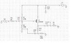
Hallo! New to this forum. ") Although my main activities involve networking and IT consulting, i am attending courses for a telecommunications postgraduate. Among the courses, there is one concerning some basic circuit designing using breadboard. The previous labs were ok, but now i am stuck in a project about common drain - source follower amplifier using a 2n5458 JFET. I have calculated all the necessary values for resistors, but i am not able to find any equations in order to calculate the value of the capacitors (Cin, Cout, Cbs, Cdc).
Although my main activities involve networking and IT consulting, i am attending courses for a telecommunications postgraduate. Among the courses, there is one concerning some basic circuit designing using breadboard. The previous labs were ok, but now i am stuck in a project about common drain - source follower amplifier using a 2n5458 JFET. I have calculated all the necessary values for resistors, but i am not able to find any equations in order to calculate the value of the capacitors (Cin, Cout, Cbs, Cdc).
Can anyone help me with it?
I also post an attachment with the spice circuit.
More info:
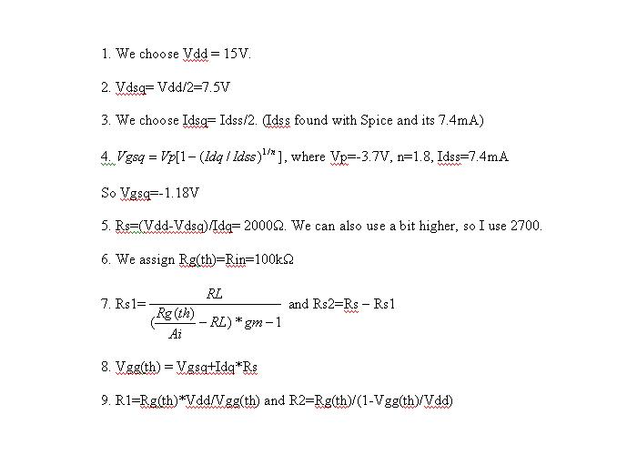
Vdd=15V. Idsq=Idss/2. Idss is 7.4mA.
Also, Ac amplitude is 25mV and we use sin values for transient analysis.
Thanks in advance.
Although my main activities involve networking and IT consulting, i am attending courses for a telecommunications postgraduate. Among the courses, there is one concerning some basic circuit designing using breadboard. The previous labs were ok, but now i am stuck in a project about common drain - source follower amplifier using a 2n5458 JFET. I have calculated all the necessary values for resistors, but i am not able to find any equations in order to calculate the value of the capacitors (Cin, Cout, Cbs, Cdc).Can anyone help me with it?
I also post an attachment with the spice circuit.
More info:
Vdd=15V. Idsq=Idss/2. Idss is 7.4mA.
Also, Ac amplitude is 25mV and we use sin values for transient analysis.
Thanks in advance.