d123
Advanced Member level 5
Hi,
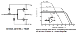
With reference to a CMOS inverter, e.g.
The CMOS Inverter Explained
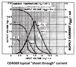
During the transition from high to low or low to high, when both P and N are briefly on, I thought there was a brief short-circuit path to ground.
Do CMOS inverters never ever need source and drain resistors to limit this current, it's only BJT push-pull stages that require emitter current-limiting resistors?
What if the gate signal were left on at mid-supply for several minutes and both P and N were on - might they be damaged?
With reference to a CMOS inverter, e.g.
The CMOS Inverter Explained
During the transition from high to low or low to high, when both P and N are briefly on, I thought there was a brief short-circuit path to ground.
Do CMOS inverters never ever need source and drain resistors to limit this current, it's only BJT push-pull stages that require emitter current-limiting resistors?
What if the gate signal were left on at mid-supply for several minutes and both P and N were on - might they be damaged?