Continue to Site

Welcome to EDAboard.com

Welcome to our site! EDAboard.com is an international Electronics Discussion Forum focused on EDA software, circuits, schematics, books, theory, papers, asic, pld, 8051, DSP, Network, RF, Analog Design, PCB, Service Manuals... and a whole lot more! To participate you need to register. Registration is free. Click here to register now.

CMOS homework.. Help!

Status
Not open for further replies.

latvian

Newbie level 3
Joined
Sep 18, 2010
Messages
3
Helped
0
Reputation
0
Reaction score
0
Trophy points
1,281
Activity points
1,306
Hello everyone,
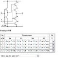
I have this question in my homework that I am having problem solving it. The question is a CMOS network of gates that I must give the truth table of it and to choose the type of the network.

The choices for the y are: 0, 1, z

The choices for the type of network is: tri-state inverter, tri-state buffer, AND network, OR network, NAND, NOR, XOR, XNOR.

The question is attached with this question as a screen shot image...

Please help!

Thanks in advance
 

Attachments

  • namnlös.JPG
    namnlös.JPG
    38.3 KB · Views: 95

A = 0, B = 0 : P1 ON P2 ON N1 OFF N2 OFF Y 1
A = 0, B = 1 : P1 OFF P2 ON N1 ON N2 OFF Y hi-Z
A = 1, B = 0 : P1 ON P2 OFF N1 OFF N2 ON Y hi -Z
A = 1, B = 1 : P1 OFF P2 OFF N1 ON N2 OFF Y hi-Z

The network seems to be NAND gate.
 

After getting two different answers, it's time to figure it out yourself, isn't it? The purpose of the homework isn't primarly to find the correct answer but to understand the problem and learn the solution method.
 

Thanks everyone for replying and helping... It's still a confusion for me....
What's a gated inverter?
 

gated inverter is a inverter controlled by gating signal
 

A = 0, B = 0 : P1 ON P2 ON N1 OFF N2 OFF Y 1
A = 0, B = 1 : P1 OFF P2 ON N1 ON N2 OFF Y hi-Z
A = 1, B = 0 : P1 ON P2 OFF N1 OFF N2 ON Y hi -Z
A = 1, B = 1 : P1 OFF P2 OFF N1 ON N2 OFF Y hi-Z

The network seems to be NAND gate.

Thank you very much for your help. I have checked the answer in our school's check system and it seems to be wrong.

Any other help would be really truly appreciated.
 

One of the comments here is true. You should understand first your homework before you answer it. Because the purpose of the homework isn't primarily to find the correct answer but to understand the problem and learn the solution method.
 

When A is low the output can only float. When it is high then the output is B inverted. So, a gated inverter, not a NAND gate.

Keith
 

A B p2 p1 n1 n2 y
0 0 off on off off 0
0 1 off off on off 0
1 0 on on off on 1
1 1 on off on on 0
 

That is incorrect. When A is low the output can only be high impedance no matter what B is.

Keith
 

Status
Not open for further replies.

Similar threads

Part and Inventory Search

Welcome to EDABoard.com

Sponsor

Back
Top