Welcome to our site! EDAboard.com is an international Electronics Discussion Forum focused on EDA software, circuits, schematics, books, theory, papers, asic, pld, 8051, DSP, Network, RF, Analog Design, PCB, Service Manuals... and a whole lot more! To participate you need to register. Registration is free. Click here to register now.
Hello, sweety
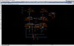
you feed gates of NMOS with rf signal - so they must be separated from bias circuitry through resistors (or chop inductors) - as in your schematic.
Just for curiosity, can you tell me smth of advantages of this schematic? Enhanced gain?
thank u...but iam not still completely getting it..in the schematic..the input ie., rf signal is feed through source...but by cross coupling we r feeding the ac signal from one source to another gate.
If the resistor is not placed..the signal which is fed from source goes to gnd instead of gate??? ....is it right ??
well...their is a degradation of NF approximately 2times compare to normal CG lna..and consumes 2 times less current..
This site uses cookies to help personalise content, tailor your experience and to keep you logged in if you register.
By continuing to use this site, you are consenting to our use of cookies.