Continue to Site
Follow along with the video below to see how to install our site as a web app on your home screen.
Note: This feature may not be available in some browsers.
The CMOS Switch even when OFF, will have some leakage. This will be worse with smaller lengths.
The amount of leakage is quite small in the order of pA to nA depending on the width and increases with temperature.
But if you are dealing with super high impedance nodes which cannot support any current, then it could be a problem. So you will need to have a larger length.
I have faced this so i know!
Hi mona123,
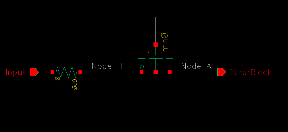
Let's assume that your switch is between a high impedance node (lets call it 'Node_h') and some other node (Node_o).
For example some low power bandgap and an Op-Amp input gate.
Now let's also assume that the Node_h cannot support ANY current, even to the order of pA.
Now without the switch, the Node_h is connected directly to Node_o which is a gate and hence there is no current drawn.
But when there is a switch between the two nodes, Node_h sees a source/drain of the switch which can leak even if the switch is turned OFF.
Normally this leakage would be quite small. But at high temperature and for large Width of the switch, the leakage can get quite large.
And this will start to load your high impedance node Node_h. And if Node_h cannot handle it, it will be screwed.
In order to reduce the leakage, you can increase the length.
The advantage here is that since you are only transmitting a voltage and not a current, you do not care about the resistance of the switch so it could be higher.
Hi nitishn5, Thanks for explaining. I am still wondering, what can go wrong from you statement "And if Node_h cannot handle it, it will be screwed". I have similar scenario. Can you please explain. Thanks for patience.
In this case you should not connect source to bulk, as the NMOS bulk usually is substrate=GND (if you don't use a double/triple well process or SOI substrate).
... use a double/triple well process or SOI substrate
But that would mean extra masks and extra cost...!
Not worth doing just for singular instances like this.