Continue to Site

Welcome to EDAboard.com

Welcome to our site! EDAboard.com is an international Electronics Discussion Forum focused on EDA software, circuits, schematics, books, theory, papers, asic, pld, 8051, DSP, Network, RF, Analog Design, PCB, Service Manuals... and a whole lot more! To participate you need to register. Registration is free. Click here to register now.

Clock offset as charge injection remedy

Status
Not open for further replies.

yefj

Advanced Member level 4
Joined
Sep 12, 2019
Messages
1,180
Helped
1
Reputation
2
Reaction score
3
Trophy points
38
Activity points
7,112
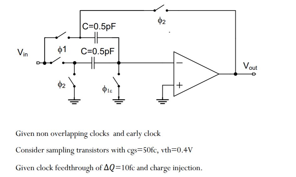
Hello,i have a switched amplifier as shown bellow the phi_epsilon switch has the same parameters as the other switch, but for simplicity no clock feed through.
i cant visualise how exacly it helps with the charge injection.
Thanks.
10.JPG
 

Phi1e is the switch that performs bottom plate sampling here.. The purpose of this technique is to mitigate the effects of non-linear charge injection. When this switch is on the charge in its channel is to a great extend independent of the input voltage being sampled, because one side of the switch is ground. Still, when you turn that switch off, there will be some charge injection that it deposits on the inverting input of the amplifier, but it is signal independent and can be eliminated with differential structures. The important thing here is that when the switch turns off the charge on the inverting input of the amplifier is frozen - ther is no ohmic path to anything. When a little bit later you turn off also Phi1 switches, they will throw terrible charge injections and the voltage at the inverting input will go crazy non-linear but the charge there will stay nice and charge injection independent, that is input signal independent. During Phi2 you flip one cap around in the feedback and the amplifier sucks all the charge from the capacitor that is connected to ground in phi2 on to the feedback cap. The total charge at the inverting input still remains the same but is now redistributed on the feedback capacitor. And this process is pretty linear. So, you basically go from voltage to charge and back to voltage.
 
  • Like
Reactions: erikl

    erikl

    Points: 2
    Helpful Answer Positive Rating
Status
Not open for further replies.

Part and Inventory Search

Welcome to EDABoard.com

Sponsor

Back
Top