Continue to Site

Welcome to EDAboard.com

Welcome to our site! EDAboard.com is an international Electronics Discussion Forum focused on EDA software, circuits, schematics, books, theory, papers, asic, pld, 8051, DSP, Network, RF, Analog Design, PCB, Service Manuals... and a whole lot more! To participate you need to register. Registration is free. Click here to register now.

Class B simulation in Cadence

Status
Not open for further replies.

AMSA84

Advanced Member level 2
Joined
Aug 24, 2010
Messages
577
Helped
8
Reputation
16
Reaction score
8
Trophy points
1,298
Location
Iberian Peninsula
Activity points
6,178
Hi guys,

I'd like to know if someone can help me simulate a Class B amplifier? From what I have seen, it is like the inverter, but in place of the PMOS (in the inverter) it has the NMOS and in place of NMOS (in the inverter) has the PMOS.

I tried to simulate but the results are not the same as in some literature that I have read.
Regards.
 

I have a Youtube video which is an animated simulation of simple class B amplifiers.

https://www.youtube.com/watch?v=nLMC8j_8ys4

Tips:

If the PNP is at the top, it gives you both voltage and current amplification. Your input can be small amplitude. However it requires careful adjustment of bias currents, in order to minimize power wastage.

If the NPN is at the top, then your input must be at the same amplitude which you desire your output to be.
 

A digital inverter switches its output high or low so each output transistor is a common-source type. An audio or video amplifier must have a linear output that can produce all voltage levels so source-follower transistors are used.
A class-B amplifier produces crossover distortion because when the signal is near halfway both output source-follower transistors are turned off. Class-AB where each output transistor is biased on a little is used for an audio or video amplifier.
Your simulation program might not know that.
 

Yeah, it is a push pull structure.You need to bias the transistors properly. In this structure, when the signal is high the NMOS will gives the gain and when the signal is low the PMOS gives the gain.
 

Thank you guys for the quick answer. The topology is to be implemented in CMOS technology with MOSFETs transistors.

The idea here is to avoid the use of the inverter, due to the simultaneous conduction. I thought that this could be a good solutions. However I have seen some other very well elaborated class B topologies. Does anyone has implemented those in CMOS tech?
 

The output transistors should be source-follower Mosfets that have NO VOLTAGE GAIN. Then the N-channel is at the positive top and the P-channel is at the ground bottom.
If you use common-source Mosfets then they produce a voltage gain and a huge current and lots of heating at halfway that changes when the temperature changes and is OK for a fast switching logic inverter but is disaster in a linear amplifier.

Maybe you are talking about designing a Cmos opamp that has low maximum output current? Then common-source Mosfets that have voltage gain can be used at the output.
 

Hi audioguru.

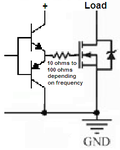
I am trying to aplly this class B topology to drive a big mosfet. The idea is to charge and discharge the big input capacitance of a transistor. The idea is precisely to inplement eome sort of inverter with very fast switching behaviour. Do you have any idea on this? Using this class B topology? In fact it would be to substitute the classical CMOS inverter. (it dissipates lots of power due to simulataneous conduction)

However one constrain that I have noticed is that this topology uses +VDD and -VSS. Can I use VSS=0V? (ground)
 

Usually a complementary pair of bipolar emitter-followers is used to quickly charge and discharge the high capacitance of the gate of a big switching Mosfet, but not in an amplifier.
A big switching Mosfet and its driver do not use a negative supply, only a positive supply.

Ordinary CD4xxx Cmos logic inverters have an output current that is too low to drive a big Mosfet quickly. 74HCxx high speed Cmos has much more output current but its max supply is only 7V which is not high enough to completely turn many high power Mosfets.
 

Attachments

  • Mosfet driver circuit.PNG
    Mosfet driver circuit.PNG
    9.3 KB · Views: 91

Thank you for your reply guru. I forgot to say that this is to be implemented on a IC. The same applies?

Moreover, since it is a synchronous converter, that is, in the case of the buck, the diode is replaced by a MOSFET and the pass device is a PMOS, I can use that drive topology for both power mosfets?
 

... one constrain that I have noticed is that this topology uses +VDD and -VSS. Can I use VSS=0V? (ground)

In schematics, very often for power supply +VDD and -VSS is shown - even for IC based circuits - because you usually need a Vref which is in the mid between, so in such case is GND.

For a real IC design, always VSS=0V , e.g. you'd have to generate Vref = VDD/2 (resistor divider + buffer).
 

At first you talked about designing a "class-B amplifier" using Mosfets at the output. Many audio power amplifiers are wrongly called class-B.
Now you are designing a completely different IC?
Sorry, I select then buy ICs, I do not design them. Ask your professor to help you.
 

Status
Not open for further replies.

Similar threads

Part and Inventory Search

Welcome to EDABoard.com

Sponsor

Back
Top