Continue to Site

Welcome to EDAboard.com

Welcome to our site! EDAboard.com is an international Electronics Discussion Forum focused on EDA software, circuits, schematics, books, theory, papers, asic, pld, 8051, DSP, Network, RF, Analog Design, PCB, Service Manuals... and a whole lot more! To participate you need to register. Registration is free. Click here to register now.

circuit with drive buffer

Status
Not open for further replies.

paardenvlees

Newbie level 4
Joined
May 14, 2020
Messages
6
Helped
0
Reputation
0
Reaction score
0
Trophy points
1
Activity points
66
Hi,

I build a circuit wit a drive buffer. When i make use of the logictoggle input from proteus the buffer(74HC365) is working correctly and when i replace them by just voltage sources and toggle the voltage source high low, it is not working anymore?

I have an output of 3.3V/0.0V from a comperator circuit and i want to use that as input to the OE. on the inputs at A1 there is also a 3.3V input.
Is this not working in proteus or what am i doing wrong?
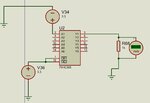

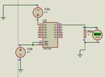
Capture.JPG
 

Hi,

I don't understand your textual explanation, nor do I understand what function you expect...

But as soon as /OE are high then the output is disabled.
Both /OE need to be LOW.

********
For a real circuit:
* you need a power supply. And the HIGH input level depends on the power supply voltage.
* no input should be left floating

Klaus
 

i mean that if i simulate my circuit with logic gates on the inputs than the buffer works normal. So low, output at Y1 is high. and high output at Y1 is low.
If i do this the same with voltage sources on the inputs the component gives alaways a low output at Y1.


Hi Stenzer,

the supply pins are correct, so this is not a problem. These are hidden but VCC is set to 5V. The component is working with the logic inputs from proteus and gives a 5V output at Y1.
See pictures below. The output with the supply voltages should also be 5V but it is 0V.
Capture.JPG
Capture1.JPG
 

Hi,

have you tried to set your supply voltage to 3.3 V? According to the TI datasheet [1], the minimum HIGH voltage level is 3.15 V @ 25 °C and V_cc = 4.5V. By having a look at the V_cc = 6 V entry, a higher HIGH level input voltage can be seen. Thus, you may expect a HIGH voltage input level larger than 3.3 V @ V_cc = 5 V.

[1] https://www.ti.com/lit/ds/symlink/cd74hct365.pdf

greets
 

Hi,

With 5V logic supply, then 3.3V input signal is not HIGH.

With CMOS logic (HC), valid high levels are 0.7V x Vcc = 0.7 x 5V = 3.5V.

--> don't use 3.3V but use 5.0V as HIGH.

And please understand that there are three output states:
* HIGH
* LOW
* Z = high impedance
 

Hi,

Unlikely - is it anything to do with source impedance/resistance so Vin at input pin is lower than what you think it should be?
 

Status
Not open for further replies.

Similar threads

Part and Inventory Search

Welcome to EDABoard.com

Sponsor

Back
Top