Welcome to our site! EDAboard.com is an international Electronics Discussion Forum focused on EDA software, circuits, schematics, books, theory, papers, asic, pld, 8051, DSP, Network, RF, Analog Design, PCB, Service Manuals... and a whole lot more! To participate you need to register. Registration is free. Click here to register now.
Normally array of caps are used for Charge pumps.
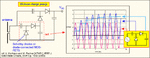
Can you please explain how the attached charge pump works?
Its not a series or cascade connection. I am confused in analysing this circuit.
I had seen some strange behaviour when I simulated chargepump (dickson) constructed using MOSFETs.
What is the switching frequency to be used? How should we select Cap value?
I have chosen 500KHz as the clock frequency and cap is 1pf.
I tried b varying the clock frequency from 250KHz to 1GHz. This charge pump is used for low power RFID applications@ 865MHz.
I am aware that there are -ve implications when we go for higher frequency. but I experimented to see the behaviour.
Moreover, I changed the width of the MOSFET from 240nm to 1um.
Strangely, I saw that as the width is increased, output is decreased. I assumed that as width of MOSFET is increased, more will be the drain current and so output voltage must be higher. Surprisingly, I found the reverse, wherein, output voltage started decreasing as the width is increased. Why is it happening so?
I changed the capacitor value from 0.01pf to 1uf. Here also, I agree that cap should be small in order to see faster response time. But still, I experimented to see the results. To my surprise, I found that as cap is increased, response time is decreased. I don't understand why is it happening so.
This site uses cookies to help personalise content, tailor your experience and to keep you logged in if you register.
By continuing to use this site, you are consenting to our use of cookies.