Continue to Site

Welcome to EDAboard.com

Welcome to our site! EDAboard.com is an international Electronics Discussion Forum focused on EDA software, circuits, schematics, books, theory, papers, asic, pld, 8051, DSP, Network, RF, Analog Design, PCB, Service Manuals... and a whole lot more! To participate you need to register. Registration is free. Click here to register now.

[SOLVED] charge pump output goes down when PMOS switch is placed in between CP and the load

Status
Not open for further replies.

allennlowaton

Full Member level 5
Joined
Oct 5, 2009
Messages
247
Helped
3
Reputation
6
Reaction score
3
Trophy points
1,298
Location
Taiwan
Activity points
3,062
Good day to all.

I would to ask for any suggestions and ideas regarding this.
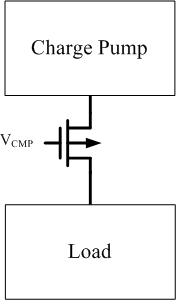
The output of charge pump without a switch is 3.85V which is already enough for my application). However, when there's a PMOS switch already
it's output become 3.25V. There's a 0.6V drop.
I want the CP output to be as high as possible.

Shown below is the figure of charge pump, switch and the load.
28_1310008707.jpg


Thank you.
 

You are not showing the bulk connection of your PMOS switch. Is its nwell connected to its source, or perhaps to a higher voltage? Is your VCMP=ON control signal low enough to fully drive the switch into triode region?
 
The bulk of PMOS is connected to its source. VCMP is either 0 or VDD.
VDD is always less than the output of charge pump.
 
Last edited:

The bulk of PMOS is connected to its source.
Ok.
VCMP is either 0 ...
Also ok.
... or VDD. VDD is always less than the output of charge pump.
Just an idea:
Is the VCMP "off" control voltage VDD - VchargePump = VGS(PMOS) possibly enough to open the switch (a little bit) during the "off" phase, so you could loose some charge pump power?

If not, I'd guess the W/L ratio of your PMOS switch isn't big enough for the charge pump current needed. So it is not large enough for this current to operate in the triode region. In order to get a low VDSsat (triode region), the switch should be designed for about the 10-fold current.
 
At VDD=2.7V, the VchargePump before the switch is placed is at 3.85V but when the PMOS switch is already present, the VchargePump drops to 3.25V. At this instance, the VCMP is at zero(0V) level to turn on the PMOS switch.

The width of the PMOS switch is the same as the switches I used in the charge pump (W=20000u, L=0.5u).

I am wondering maybe the VchargePump droop is caused by connecting the source terminal of the PMOS switch to the output of the charge pump. As we know, the source terminal has a low impedance equivalent.
 

... maybe the VchargePump drop is caused by connecting the source terminal of the PMOS switch to the output of the charge pump. As we know, the source terminal has a low impedance equivalent.

That's what it should have. The connection and control of your PMOS switch is quite ok. I suspect the W/L ratio of your charge pump and switch transistor(s) (40000) is still too low for your current needs (load). Try and enlarge these ratios (analyze by simulation) and see if your voltage output gets higher.
 
  • Like
Reactions: allennlowaton

    V

    Points: 2
    Helpful Answer Positive Rating

    allennlowaton

    Points: 2
    Helpful Answer Positive Rating
I did a simulation using a very large switch PMOS device. The result is still the same. It fails.
 

I did a simulation using a very large switch PMOS device. The result is still the same. It fails.

Did you also increase the charge pump transistors? May be the PMOS switch device (from the charge pump to the load) is large enough, but the output impedance of your charge pump is too low?
 
I changed the size of the switch which connects the charge pump to the VDD. The circuit is now properly working. thanks..
 

Status
Not open for further replies.

Part and Inventory Search

Welcome to EDABoard.com

Sponsor

Back
Top