Continue to Site

Welcome to EDAboard.com

Welcome to our site! EDAboard.com is an international Electronics Discussion Forum focused on EDA software, circuits, schematics, books, theory, papers, asic, pld, 8051, DSP, Network, RF, Analog Design, PCB, Service Manuals... and a whole lot more! To participate you need to register. Registration is free. Click here to register now.

charge pump - can presented topology replace for the PMOS?

Status
Not open for further replies.

crazyfox

Junior Member level 2
Joined
May 12, 2007
Messages
23
Helped
0
Reputation
0
Reaction score
0
Trophy points
1,281
Activity points
1,452
charge pump

16_1251173066.jpg


HI :

I have a question for a charge pump circuit

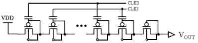
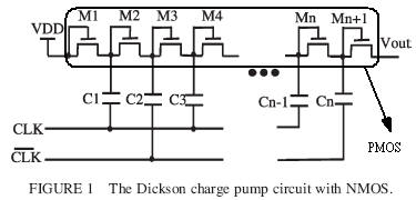
The topology shown in FIg1. with NMOS can replace for the PMOS ?

It seems no used with PMOS ?

Thanks .
 

charge pump

Those FETs are just opportunistic diodes, a plain P-N or
a PMOS would be as functional but PMOS has poorer
specific on-resistance. Just get your gate tied to the right
side.

Of course well parasitics might not be in your favor, you
would have to see what your well voltage range and your
well-tie options are.
 

Re: charge pump

Thanks for your reply,

from simulation results it seems function work with PMOS, but when really used

it cannot pump the voltage up, and have large leakage current.

I still cannot find the reason for the phenomenon.

Thanks.
 

charge pump

If PMOS NWell is tied to VDD, then PMOS S/D can't
go more than a Vf above that without conducting. You
need the NWell to float with each PMOS source
individually. This is what I mean about the parasitic
elements being unfavorable. If you have an HV N-well
or SOI process you might be able to do it; an N-epi,
single PWell process and you're hosed.
 

Re: charge pump

60_1251257511.jpg


Thanks for your reply,

The PMOS device use HVNWELL, and it is my circuit.

I think it is what you mean, but the circuit have the leakage problem.

thanks
 

Re: charge pump

I don't like the looks of that, you want MOS conduction
but body diode conduction is a bad idea because there
is at least a BJT, maybe an SCR in the basement.

G=D=cathode, B=S=anode I think you want. And check
the polarities in a simple circuit to satisfy yourself about
the diode qualities as-hooked-up.
 

    crazyfox

    Points: 2
    Helpful Answer Positive Rating
Re: charge pump

Thanks for your suggestion.
 

Status
Not open for further replies.

Part and Inventory Search

Welcome to EDABoard.com

Sponsor

Back
Top