Continue to Site

Welcome to EDAboard.com

Welcome to our site! EDAboard.com is an international Electronics Discussion Forum focused on EDA software, circuits, schematics, books, theory, papers, asic, pld, 8051, DSP, Network, RF, Analog Design, PCB, Service Manuals... and a whole lot more! To participate you need to register. Registration is free. Click here to register now.

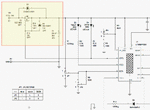
Cant understand what this part of the circuit does

Status
Not open for further replies.

electrophile

Member level 2
Joined
Aug 30, 2013
Messages
48
Helped
1
Reputation
2
Reaction score
1
Trophy points
1,288
Activity points
1,677
Hi, Can anyone please help me understand this circuit (see the attached PDF. The part I cant understand is in the red box in the top left corner). Is this some sort of power-path control? This is basically a Li-Ion battery charger. The MOSFET seems to be controlled by the CHRG pin which goes low when charge is complete and otherwise stays high. The high and low on this pin are logic levels. I tried simulating this in LTSpice IV (also attached) but couldnt really understand what it does. This part is actually optional but I'd still like to know what it does. Any help would be appreciated. Thanks!

MODERATOR ACTION: I'm attaching the relevant part of the schematic in gif format for faster access
Snap1.gif
 

Attachments

  • LT3652HV Demo Schematic 2.zip
    75.8 KB · Views: 57
Last edited by a moderator:

It seems to me it's used to lower the input voltage drop that is to decrease the loose of power, especially for high currents.

The diode CMSH3-40MA has a voltage drop of about 0.45 V for a current of roughly 2A; in this case 0.45*2=0.9W are lost.
The mosfet Si2319DS has a Rds(on) of about 0.08 ohm that means the lost power is 0.08*2^2=0.32W.
 
The high and low on this pin are logic levels.
No. CHRG is a 40V rated open collector output, otherwise the circuit won't work.
 

@albbg - Thanks. Yes thats what that does. It reduces power drop across the blocking diode to increase charger efficiency. I found a document after I posted here that explains this.

@FvM - My bad. The pins are binary coded but not logic levels. You are right. They can accept voltages as high as Vin.
 

I think it is used for reverse polarity protection .
 

I assume R14 increases stability, and D9 prevents exceeding VGSmax. I have no idea what R13 is for though, perhaps someone else can comment on that?
 

Quite simple.
As said, CHRG is open collector, so there must be a pull-up resistor R14.
Voltage limiting z-diode can hardly work without current limiting R13.
 

Status
Not open for further replies.

Similar threads

Part and Inventory Search

Welcome to EDABoard.com

Sponsor

Back
Top