Continue to Site

Welcome to EDAboard.com

Welcome to our site! EDAboard.com is an international Electronics Discussion Forum focused on EDA software, circuits, schematics, books, theory, papers, asic, pld, 8051, DSP, Network, RF, Analog Design, PCB, Service Manuals... and a whole lot more! To participate you need to register. Registration is free. Click here to register now.

can't get chipscope to work.

Status
Not open for further replies.

laserbeak43

Member level 1
Joined
Aug 15, 2008
Messages
33
Helped
1
Reputation
2
Reaction score
1
Trophy points
1,288
Location
Maryland, USA
Activity points
1,491
Hello,
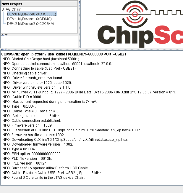
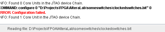
I'm using Chipscope and the ISE 10.1 suite and i can't get it to work.
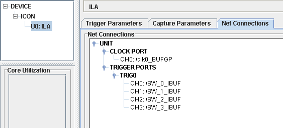
ERROR:ChipScope: One or more invalid signal connections detected.
ERROR:ChipScope: Double-click the scope.cdc icon in the sources window to edit and fix the CDC project.
ERROR: Chipscope Insertion failed
I'm using some very simple code
Code:
module two_input_xor (
	input wire in1,
	input wire in2,
	output wire out
	);
	assign out = in1 ^ in2;
endmodule
and this doesn't even work. I've read xilinx's chipscope doc and decyphered what i could, but it still left me googling for tutos and i still get the same results after reading this one **broken link removed**

can someone please help?
 

HI
this message comes when all signals are not assigned clock and triggers properly...
if u run your .cdc files,the unconnected signals highlights in red color check out...
y


i hope this helps u...
 

The fact that the "very simple code" hasn't a clock may be reason enough for failure. You should try with a
somewhat elaborated code, e.g. a counter.
 

Hi
thanks for the reply, I kind of gave up on chipscope. seems like just another xilinx headache. but you've inspired me to keep trying.
This is my new module and it synthesizes with no errors
Code:
module clockedSwitches(input clk0,
							input [3:0] SW,
							output [3:0] LEDR
    );

	parameter ms5 = 18'd250000; 
	reg [17:0] cnt; 
	reg [3:0] LED;
	always @(posedge clk0)
	begin
		if(|cnt) cnt <= cnt-1;
		else
			begin
				cnt <= ms5;
				LED <= SW;
			end
	end

	assign LEDR = LED;
	
endmodule
This Picture shows that my connections are good.

i click Analyze Design Using Chipscope and I get these warnings during implementations and Program file generation processes

WARNING:par:288 - The signal U_ila_pro_0/U0/I_NO_D.U_ILA/U_STAT/iSTAT<11>_wg_lut<7> has no load. PAR will not attempt
WARNING:Route:455 - CLK Net:icon_control0<0> may have excessive skew because
WARNING:par:283 - There are 1 loadless signals in this design. This design will cause Bitgen to issue DRC warnings.
WARNING:physDesignRules:367 - The signal

and this is what happens when chipscope is started
1st, everything SEEMS good


but when i configure i get this error:


can someone please help? I just ordered a crap load of peripherals for my board too. It kind of stinks...
 

Can you show us the full code where the ila and the icon blocks are instantiated along with your functional code?

r.b.
 
that is the full code. i just tried to make something that chipscope could use.
 

You need to generate ILA and ICON Verilog or VHDL blocks using Coregen and then build these into your project as well as your functional code.

Chipscope requires these blocks, as they sample the signals you are interested in and send the data to the Chipscope software.

r.b.
 

i used the inserter. as i was told that was the only method i needed to use. are you sure i need to generate cores?
 

The only way I have ever done it is to instantiate the ILA and ICON cores in my code. The inserter has never worked well for me.
 

Status
Not open for further replies.

Part and Inventory Search

Welcome to EDABoard.com

Sponsor

Back
Top