Continue to Site

Welcome to EDAboard.com

Welcome to our site! EDAboard.com is an international Electronics Discussion Forum focused on EDA software, circuits, schematics, books, theory, papers, asic, pld, 8051, DSP, Network, RF, Analog Design, PCB, Service Manuals... and a whole lot more! To participate you need to register. Registration is free. Click here to register now.

Can't apply over 50 volts to h-bridge

Status
Not open for further replies.

muyil

Newbie level 4
Joined
Oct 29, 2020
Messages
7
Helped
0
Reputation
0
Reaction score
0
Trophy points
1
Activity points
40
Hi Everyone,

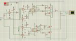
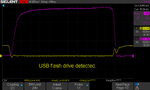
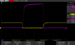
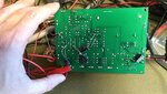
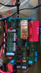
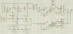
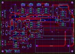
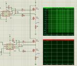
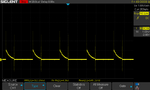
I have been testing my inverter design recently. I tried to apply 150V to h-bridge as a bus voltage but it started to pull a lot of current and the 150V dropped down to 50 volts. The circuit doesn't pull much current below 50 volts. Why could this be happening? I am using ir2110 driver IC and didn't apply any dead time. Could this be the problem? If so, how can I solve that? It works well with the simulation as well.

Regards
 

Attachments

  • Untitled5.jpg
    Untitled5.jpg
    782.7 KB · Views: 166
  • SDS00031.png
    SDS00031.png
    14.7 KB · Views: 184
  • SDS00032.png
    SDS00032.png
    14.4 KB · Views: 149

Hi,

not the best design. I see a lot of issues.

But I guess the overcurrent is caused by an inappropriate inductance.

Did you simulate it´s currents?
What´s the saturation current for the real device?

Klaus
 

Hi,

not the best design. I see a lot of issues.

But I guess the overcurrent is caused by an inappropriate inductance.

Did you simulate it´s currents?
What´s the saturation current for the real device?

Klaus

Hi Klaus,

I didn't simulate it's current. I removed IR2110 which drives 50 khz signal to mosfets. Then I could manage to increase the dc bus voltage up to 340 volts. But when I removed IR2110 which drives 50 hz signal to mosfets, I had over current problem. It's the same problem when I test whole circuit. So I consider problem is due to 50 khz switching. But this happens only when I apply over 50 volts.
 

Hi,

your schematic seems to be from a simulation tool.
So it should be easy to simulate the current.

Dead time problem can be simulted, too. Just show draw the MOSFET currents of one half bridge in one chart.

But now I read thet there still is an overcurrent problem, when the IR2110 are removed. If so, where does the current flow? Due to the gate resistors all MOSFETS should be OFF then.

I still don´t know what inducatance you use. Please post a link to it´s datasheet.

Klaus
 

Everything works fine with simulation. I can't measure the current passing through the mosfets. Simulation program doesn't allow me to do so. I removed output capacitor and inductor from pcb. Still has the same problem.
 

I removed output capacitor and inductor from pcb. Still has the same problem.
As long as the devices are not killed this is impossible.

Please show photos of both sides of the PCB with all the wiring.

Klaus
 

Here they are
 

Attachments

  • untitled1.jpg
    untitled1.jpg
    61.8 KB · Views: 148
  • Untitled2.jpg
    Untitled2.jpg
    128.1 KB · Views: 169
  • Untitled3.jpg
    Untitled3.jpg
    1.6 MB · Views: 174

So,

I see no
* true GND plane
* bulk cap at the high voltage
* I see no fast decoupling cap at high side MOSFET drain.
* bulk capacitor for the 12V
* fast decoupling capacitor at each 12V pin of each IC, especially close to D3 and D4
* resonance suppression at the output LC filter
* noise suppression capacitor at the reference voltages
* sufficient isolation for the high voltage

This does not mean that the circuit fails from the first power ON. But it´s likely that one or more issues cause a fail at higher voltages. Maybe even kills your MOSFETs or your drivers.

The pictures are good, but I can´t follow the signals. It´s too complex and takes a lot of time.
Do you have PCB plots from your PCB software?

A power swtiching application is no simple application. It needs to take care of high voltages, high currents fast edges....

Klaus
 

Is it that one ?
 

Attachments

  • Untitled6.jpg
    Untitled6.jpg
    1 MB · Views: 174

Hi,

D3 and D4 are extremely overdimensionated. A small 1A schottky is more than sufficient. It won´t even get warm.
But they need to withstand your high voltage plus ringing. So in a good design a 200V type should be sufficient.
--> Because yours withstand 600V I see no problem.

Klaus
 

Hi Klaus,

I added 1 ohm resistors under the half bridges to measure the current. The high frequency(50khz) side has current peaks up to 5.5A. On the other hand, the 50 hz side has no current peaks as it should, meaning they are never ON at the same time. So does this current peaks also mean both mosfets are ON some amount of time?
 

Attachments

  • Untitled9.jpg
    Untitled9.jpg
    804.7 KB · Views: 167

This is how it looks like on oscilloscope(real test). The output voltage of my push-pull converter drops down to 40VDC from 150VDC and supply voltage of the push-pull converter pulls 5A from power supply. So 60W is dissipated.
 

Attachments

  • SDS00034.png
    SDS00034.png
    16.7 KB · Views: 157

I added 1 ohm resistors under the half bridges to measure the current. The high frequency(50khz) side has current peaks up to 5.5A. On the other hand, the 50 hz side has no current peaks as it should, meaning they are never ON at the same time. So does this current peaks also mean both mosfets are ON some amount of time?
Sounds like a reasonable guess. The complementary LM339 topology provides some systematic dead time by asymmetrical propagation delay, but it may be dwarted by comparator offset voltage and delay variations. I'm not sure if too small dead time is the reason for the observed problems, but this can be best checked by increasing dead time.
--- Updated ---

Some post #7 schematic details don't look real, e.g. 75R + 100 nF "snubber". Due to variations between different schematics, I'm not sure which corresponds to the actual circuit.
 
Last edited:

put reverse shottkies ( 35V 1A ) across the 10 ohm GD resistors to speed the turn off and give more dead time - most of your issues may well be RFI from the circuit as Vdd is increased - try upping the 10R to 47R and seeif things improve - make sure your mosfets are well heatsunk ....! - if the layout is poor the centre of the totem pole can go below gnd and really upset 2110 drivers ...
--- Updated ---

Also - your snubber caps are way too big, the leads on the electro's on the underside of the pcb should be as short as possible, there is no guarantee of suitable dead time with the gate drive generation circuitry ...
 

Status
Not open for further replies.

Similar threads

Part and Inventory Search

Welcome to EDABoard.com

Sponsor

Back
Top