Continue to Site

Welcome to EDAboard.com

Welcome to our site! EDAboard.com is an international Electronics Discussion Forum focused on EDA software, circuits, schematics, books, theory, papers, asic, pld, 8051, DSP, Network, RF, Analog Design, PCB, Service Manuals... and a whole lot more! To participate you need to register. Registration is free. Click here to register now.

Can anyone plz tell me how to calculate internal impedance of a circuit?

Status
Not open for further replies.

anushaas

Member level 5
Joined
Jan 4, 2011
Messages
84
Helped
0
Reputation
0
Reaction score
0
Trophy points
1,286
Activity points
1,979
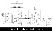
I have an amplifier circuit involving two opamps(LMC662C and OP07),resistors and capacitors.can anyone tell me how to calculate the internal impedance of the circuit

---------- Post added at 05:48 ---------- Previous post was at 05:39 ----------

This is the circuit
 

It is not evident what you mean by 'internal impedance'. Do you mean the input or the output impedance?
What is the circuit intended to do?
Prof78
 

    V

    Points: 2
    Helpful Answer Positive Rating
It is not evident what you mean by 'internal impedance'. Do you mean the input or the output impedance?
What is the circuit intended to do?
Prof78

It is an amplifier circuit with a current input of range 1pA to 1 nA.But I don't have a source of that range.So I thought of providing a shunt resistance to it so that my source generating 1nA will allow some current in the pA range to the circuit giving an output voltage in the range 0-5V.Hence I need to find the internal resistance of this circuit
 

Well, the input resistance is roughly 200k ohms but if you are amplifying a current then the input resistance should be as low as possible and the first stage should be a transimpedance amplifier. Remove the 200k resistor.

Keith
 
It is an amplifier circuit with a current input of range 1pA to 1 nA.But I don't have a source of that range.So I thought of providing a shunt resistance to it so that my source generating 1nA will allow some current in the pA range to the circuit giving an output voltage in the range 0-5V.Hence I need to find the internal resistance of this circuit

Where is the "shunt resistance"?
Again, you repeat the phrase "internal" resistance. However, I think the interpretation of Keith is appropriate. (It's bad if we have to interpret your wording).
If you need pico-amps instead of nano-amps at the input of the transimpedance configuration (as Keith has proposed), in principle you can apply current division (analog to voltage division).
 

    V

    Points: 2
    Helpful Answer Positive Rating
The replies from Keith1200 and LvW will underline why I asked my original question. What you are asking about is the input impedance of the circuit not the internal impedance. The function of the input resistor (like your R1) in the more common inverting opamp circuit for amplifying voltage inputs is to convert the voltage signal to a proportional current, remembering that the summing junction is a ‘virtual common’. If you already have a current as input then you do not need R1 and the circuit is then known as a transimpedance amplifier. The input current flows through the feedback resistance (your R2 and R3) to give an output voltage V=I(in) x (R2+R3) and the ‘transimpedance gain’ is just (R2+R3) ohm. The input impedance is effectively zero i.e. that of the virtual common. For a quick outline of the design procedure for such amplifiers see for example the article by R A Pease:
**broken link removed**

since there are a number of design matters to be considered and you must take these into account. If you wish to operate at input current values of pA then the values for R2+R3 you have used are rather low and will only give you an output of 2microvolt for 1pA input. You should in general use the highest value of feedback resistor i.e. transimpedance gain you can within the limit of the bandwidth you require, which is set by the feedback resistor and your C1 feedback capacitor, though there are techniques for extending this. The higher the transimpedance gain the better the signal-to-noise ratio. Some have difficulty in understanding this but particularly at very high gain where the main contribution to the noise is the Johnson noise of the feedback resistor then the signal increases proportional to the resistor while the noise increases as only the square root of the resistor value.
A secondary comment is that the resistor R5 is the load resistor for the LMC662 and is rather too low at 20ohm.
An alternative way of generating small input currents (and which will also allow you to see the transient response) is to use the charging current for a small capacitor. Connect a function generator providing a triangle wave to the input through a small (good quality) capacitor. Then since for capacity C with charge q and voltage v:
C = q/v or q = Cv then dq/dt = C(dv/dt)
Since the C charging current i = dq/dt, then i = C(dv/dt)
Thus if you have a triangle wave, for which dv/dt is fixed during one half of the triangle wave then you will get a constant charging current i. When the triangle wave reverses in slope the current will be the same magnitude but of opposite sign and the amplifier output should be a squarewave. So by adjusting the slope of the triangle wave ( frequency and amplitude) and choosing the appropriate C you can get any current you require.

Prof78.
 

It is an amplifier circuit with a current input of range 1pA to 1 nA.But I don't have a source of that range.So I thought of providing a shunt resistance to it so that my source generating 1nA will allow some current in the pA range to the circuit giving an output voltage in the range 0-5V.

The transconductance of the circuit is 10V/nA, so you won't get 5V with pA input anyway. It's however easy to reduce the gain of the circuit.

Another issue is brought up by the high voltage gain of the circuit. With open input or a true current source connected, the LMC662's +/- 3 mV offset voltage will be "only" multiplied by the factor 500 gain of the second stage, resulting in up to +/- 1.5V output offset. By connecting a shunt to the input, the overall gain is multiplied by the factor 100 voltage gain of the first stage, so the LMC662 offset voltage will cause the second stage to saturate immediately. In other words, it doesn't work.
 
Sir
I tried the above circuit but I could not get an appropriate output voltage in the range 0-5V.
The output voltage was constantly 11.78 volt.

I used a voltage source in the mV range along with 1 Giga Ohm input resistance so that I can get some 1 to 10 pA current input to circuit.

Can you kindly suggest improvements if any that has to be made to the circuit so as to get the desired output(0-5V).
 

Did you remove the 200k input resistor? If not then you will just saturate the output by amplifying the offset of the first opamp.

Did you really build this or did you simulate it? If you built it, where did you get the Giga ohm resistor? If you simulated it then why not use a current source for the input?

Keith

Yeah.I removed the 200k input resistor.I built the circuit.1Giga Ohm resistor was available in our lab
 

you have most likely blow up the LMC662
The first OP stage can be tested separately to check, if it's still alive (after reducing it's power supply).
 
LMC6062 is deigned for a maximum (single) supply voltage of 15V. It will be damaged with +/- 12 V.

It is given in the datasheet under absolute maximum ratings that Supply Voltage (V+ − V−) is 16V.What does that mean?

---------- Post added at 01:44 ---------- Previous post was at 01:34 ----------

The Si PIN photodiode S5972 from Hamamatsu is found to have a typical dark current of 0.01nA(10pA).Can I use this as a picoampere source?.How can I find the R and C values for such a photodiode circuit ?
 

Supply Voltage (V+ − V−) is 16V.What does that mean?
What it says, a difference. E.g. in your case, +12V - -12V = 24 V (> 16V!)
The Si PIN photodiode S5972 from Hamamatsu is found to have a typical dark current of 0.01nA(10pA).Can I use this as a picoampere source?.How can I find the R and C values for such a photodiode circuit ?
I know, that the Hamamatsu datasheets have much more detailed information, e.g about capacitances and parallel resistance.

Generally, I wonder what you want to achieve. The circuit doesn't look like a well considered picoampere amplifier. Particularly the rather low current sense resistor and the high voltage gain are causing a lot of problems. I would expect > GOhm feedback for a sensitive I/V converter.

The objective of your test is even more unclear.
 

The first OP stage can be tested separately to check, if it's still alive (after reducing it's power supply).

Sir,

I checked the first stage (LMC662 alone) separately, giving +5V and -5V supply to the IC(Used a new IC this time).The output was 4.99.Output was 3V for +_3V input.The output was more or less same as input in all cases.

Can anyone tell me what could be wrong?

---------- Post added at 10:49 ---------- Previous post was at 10:35 ----------

What it says, a difference. E.g. in your case, +12V - -12V = 24 V (> 16V!)
Thank you

I would expect > GOhm feedback for a sensitive I/V converter.


.
I tried the circuit with 1GigaOhm feedback resistance as well(Maximum R available in my lab).Still the output was nearly the same as input(say 4V o/p for input of +4V and -4V to LMC662)
 

Can anyone tell me what could be wrong?
Nothing that can be seen from your schematic diagram.
I tried the circuit with 1GigaOhm feedback resistance as well
Yes, the value sounds more reasonable. But the observed problem won't be related to feedback resistor value. Did you check the correct connection of OP input pins, and also for any hidden shorts with an ohmmeter?
 

I checked the first stage (LMC662 alone) separately, giving +5V and -5V supply to the IC(Used a new IC this time).The output was 4.99.Output was 3V for +_3V input.The output was more or less same as input in all cases.

I tried the circuit with 1GigaOhm feedback resistance as well(Maximum R available in my lab).Still the output was nearly the same as input(say 4V o/p for input of +4V and -4V to LMC662)

Anushaas, I wonder if I understand you correctly:
Did you connect a VOLTAGE source directly to the inverting input of the opamp (that is intended to be used as a I-V convertor?)
 
  • Like
Reactions: FvM

    FvM

    Points: 2
    Helpful Answer Positive Rating
Anushaas, I wonder if I understand you correctly:
Did you connect a VOLTAGE source directly to the inverting input of the opamp (that is intended to be used as a I-V convertor?)

Oh no.The input resistance was 1Gohm at the inverting input.Supply was given to pins 4 and 8(V- and V+ pins)

 
Last edited:

OK, in this case it was a misunderstanding (bad wording on your side).
As you have seen, the quiescent output is at app. 10 mvolts. Can you live with this?
Of course, this is the reason for the surprising behaviour of the ouput signal (decreasing voltages for increasing input).
By the way (in order to avoid misunderstandings): You should not use the phrase "supply voltage" for the input signal.
LvW
 
Last edited:

Status
Not open for further replies.

Similar threads

Part and Inventory Search

Welcome to EDABoard.com

Sponsor

Back
Top