Continue to Site

Welcome to EDAboard.com

Welcome to our site! EDAboard.com is an international Electronics Discussion Forum focused on EDA software, circuits, schematics, books, theory, papers, asic, pld, 8051, DSP, Network, RF, Analog Design, PCB, Service Manuals... and a whole lot more! To participate you need to register. Registration is free. Click here to register now.

Can anybody explain the meaning of this DRC error?

Status
Not open for further replies.

mfhanif

Junior Member level 2
Joined
Jan 11, 2007
Messages
23
Helped
0
Reputation
0
Reaction score
0
Trophy points
1,281
Activity points
1,451
DRC error

Hi,
I have auto generated layout from the schematic; while running the DRC i am getting "Nmos to pwell contact max 30um"..... can anybody explain the meaning of this error ....

thanks
 

Re: DRC error

looks to me as if you dont have a substrate tie going around the module.
 

Re: DRC error

k_90 said:
looks to me as if you dont have a substrate tie going around the module.

whats the suggestion ??
 

Re: DRC error

add a substrate tie as close to the nmos as you can. There may be an option to add a substrate tie to the transistor in its properties menu (depending on the quality of the tech files from the foundry, AMS c35 has them).
 

Re: DRC error

hi,

for every device there is max device width and when the device crosses this max width it flags a drc error like yours i.e. nmos to pwell contact distance is 30um.

as your device is nmos, the substrate tie for it is ptap or ptap ring and for pmos it is ntap or ntap ring.

to clear this drc error place ptap or p-guard ring(ptap ring) very close to the device, you can put devices inside this ring. in this way the source and drains of the devices can encounter the substrate tie very close to it and your error will be cleared.

Paramjyothi
 

Re: DRC error

Paramjyothi said:
hi,

for every device there is max device width and when the device crosses this max width it flags a drc error like yours i.e. nmos to pwell contact distance is 30um.

as your device is nmos, the substrate tie for it is ptap or ptap ring and for pmos it is ntap or ntap ring.

to clear this drc error place ptap or p-guard ring(ptap ring) very close to the device, you can put devices inside this ring. in this way the source and drains of the devices can encounter the substrate tie very close to it and your error will be cleared.

Paramjyothi


i believe Saint's book IC Layout Basics has a brief explanation about it.
 

Re: DRC error

more subtrate tied near your device
 

DRC error

Hi,

Any DRC will check as per the minimum distances and minimum dimensions to be followed for DRC Clean. Thus with error "Nmos to pwell contact max 30um"..... which states that the distance between the NMOS device and a substrate Pwell contact must not exceed 30um and place them close to each other.

regds,
anup
 

Re: DRC error

this error tells that the space between your substrate contacts is exceeding 30um.

generally foundary specifies the distance upto which a substrate contact is effective, in your case it is 30um...i.e some of your devices are placed more that 30um away from the substrate contact.

this error if ignored, can become a reason to cause latchup in your design.
 

Re: DRC error

mfhanif said:
Hi,
I have auto generated layout from the schematic; while running the DRC i am getting "Nmos to pwell contact max 30um"..... can anybody explain the meaning of this error ....

thanks

Place a psub contacts or guardring around the nmos...it seem that there's no psub contacts near the nmos and the rule said that if it doesn't see any psub contacts with a max distance of 30um in any nmos then DRC will complain.
 

Re: DRC error

i mdae layout of inverter in UMC 90 nm technology.. whern i run DRC it's showing many errors like ..
metal 1 coverage must be larger than 20% over lacal 100um*100um area step 50um
this error is showing upto metal 11.. there is one another error is coming... Die corner rule 1, ME! must draw with 135 angle.... plz help me... its very urgent for me..... plzzzzzzzzzzz
 

Re: DRC error

lokesh garg said:
i mdae layout of inverter in UMC 90 nm technology.. whern i run DRC it's showing many errors like ..
metal 1 coverage must be larger than 20% over lacal 100um*100um area step 50um
It is M1 density error. Your need to fill more M1. (which i doubt in inverter) probably your instance layer is not at proper place and size.

lokesh garg said:
this error is showing upto metal 11..
you can ignore this error after metal1 bcause ( I assume) you are using only upto metal 1.

lokesh garg said:
there is one another error is coming... Die corner rule 1, ME! must draw with 135 angle.... plz help me... its very urgent for me..... plzzzzzzzzzzz
I believe only orthogonal connection is allowed in umc except in chip corners.you might have used non orthogonal connection sumwhere.check.
 

Hello,

I have auto generated layout from the schematic; while running the DRC i am getting "Nmos to pwell contact max 30um"..... can anybody explain the meaning of this error ....

The meaning of this error is that your transistor NMOS have four contacts :gate,drain,source and bulk.The contact of Bulk is in the pwell.So the max distance between contact transistor(drain or source) and pwell contact is 30µm.

I hope that is the answer of your question.

what is your auto generated layout software ?
Can you help me by giving any documentation or this software.

Thank you for help
 

I menas you have either not place subsy=trate contacts in your layout or the distance between them should be less than 30u
 

Sorry, many discussions, all correct, however beating around the bush!

Yeah, I've observed similar [long back though].
Unless instructed, Virtuoso-XL does not place NTAP PTAPs.

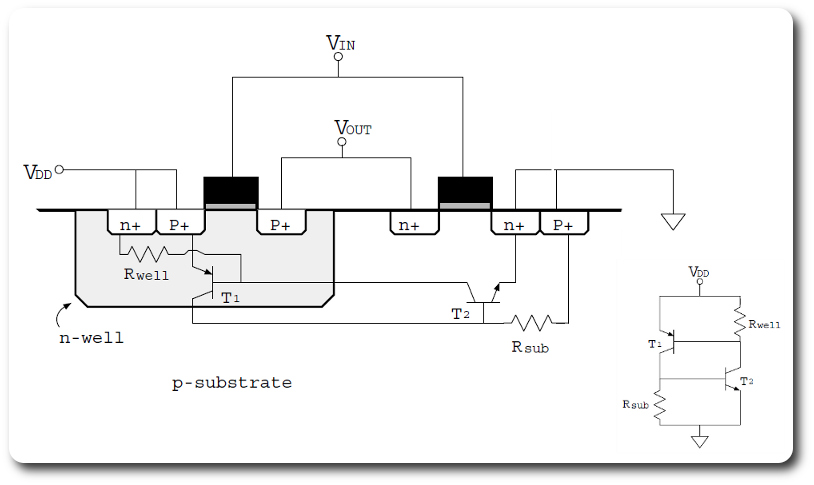
Placing a PTAP anywhere in the same PWELL [PSUB] is going to establish electrical connection to the bulk terminal of the MOS, and it does pass LVS too. However Well TAPs too far from MOS cause latchup problems in CMOS in general.

33_1262859264.jpg


All you need is Rwell, Rsub, to be small enough to prevent such. Unlike other DRC separation checks, where layers or objects are checked to satisfy a minimum separation criteria, the Latch-Up problem is checking for maximum distance criteria.

The max distance depends on substrate bulk resistivity [native doping density] and wafer type [111, 110, bulk, epitaxy] as well, hence this distance might be different for MS process versus Logic versus MS-RF foundry process, even in the same process node.

For SOI this is not required!
 

Status
Not open for further replies.

Part and Inventory Search

Welcome to EDABoard.com

Sponsor

Back
Top