Welcome to our site! EDAboard.com is an international Electronics Discussion Forum focused on EDA software, circuits, schematics, books, theory, papers, asic, pld, 8051, DSP, Network, RF, Analog Design, PCB, Service Manuals... and a whole lot more! To participate you need to register. Registration is free. Click here to register now.
Hi,
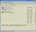
when I do the Calibre exam, I confused with a DRC error-------GR594, does anybody know how to correct it? By the way, I use IBM .13um.
ths very much.
Looks like an Antenna Rule violation: the M2 area (cf. the given 56-Vertex M2 polygon) is too large (> 20%) in relation to the connected pMOS S/D implant area, I guess.
To avoid it, you could either
insert layer hopping (M2 - Mx - M2 , x=(1||3)) between the interior (S-)taps
or
increase the associated p+ implant (S resp. D) area.
Perhaps you might find an explanation of the GR594 violation in your PDK docu?
Hello,
thanks for your explaintion. I just get over this problem. Do you know how I did it? Neither insert layer nor the area, which I try first is not avilialbe, I just decrease the vias from the NW to M1, just leaves 1/4 of the orginal. I don't know why to do this, but which is very useful.
This site uses cookies to help personalise content, tailor your experience and to keep you logged in if you register.
By continuing to use this site, you are consenting to our use of cookies.