Continue to Site

Welcome to EDAboard.com

Welcome to our site! EDAboard.com is an international Electronics Discussion Forum focused on EDA software, circuits, schematics, books, theory, papers, asic, pld, 8051, DSP, Network, RF, Analog Design, PCB, Service Manuals... and a whole lot more! To participate you need to register. Registration is free. Click here to register now.

Cadence Virtuoso layout problem !

Status
Not open for further replies.

Ata_sa16

Full Member level 6
Joined
Mar 29, 2016
Messages
343
Helped
59
Reputation
118
Reaction score
58
Trophy points
28
Location
Milky Way Galaxy, 179° 56′ 39.4″
Activity points
2,221
Hi all,

I have a problem in layout design.

I have a capacitor in my schematic and when I start doing layout I do generate all from source.

I want to do "flatten" and modify the layout of that capacitor.
I do it and make new cell and save it.

Now, the problem is when I do this, layout and schematic does not match and it does not show the connection anymore. In the schematic, it is named mim_cap however in layout it is new cell.


how can I solve this problem ???

Thank you all for your time.
 

I'd start with making sure that all layers are made
visible and selectable. When you explode an instance
then all of the "loose polygons" have to be selected
to make the "make cell" have the same contents as
original (only fixed geometry). You may have a bunch
of "residue" that you can't see and can't select,
under your new cell. Stuff that perhaps the extract
rules key on.

Also may want to play with "preserve pins" if the
particular PDK extract scheme needs those to
figure connectivity, rather than using layout-layer
recognition logic.
 

sure looks like a layer issue. mimcap devices usually have non-drawing layers 'under' them so LVS can recognise the component correctly
 

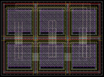
I have a cap with 6 multiplier and when I generate from source it gives me this :

cap1.png

I dont need NWELL and DNW under my caps since I will connect their bulk to PSUB so I erase NWELL and make them compact and It becomes like this:

cap2.png

and I make it new cell with new name.

How can I replace this with previous cap and not have LVS error ??!**broken link removed**
 

Why can't you create a new schematic that matches the modified design?
 

I think you're wrong to eliminate the NWell features,
they may be part of how the MIM cap is expected to
look, codified in the extract rules. You could experiment
with this step by step, and see whether a simple flat
polygons-equivalent cell also fails.
 

No I am not wrong. Nwell is used for Bulk connection. Why would we use Nwell for capacior if we want to connect its bulk to psub ???

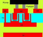
capacitor means 2 metal layers.

quest_fig1.jpg

- - - Updated - - -

But anyway forget about this. Imagine, I made a manual sub-layout and I want to use it in my main layout. How can I define this new cell in my schematic in order to not to have LVS errors ???
 
Last edited:

The MIM cap has no bulk connection. But its model
netlisting wants to attach the "bottom plate to X"
capacitor's other terminal to something, and you
changed the "something" to something that has now
gone away. So not surprising that you broke the
extract logic. Many PDKs have hard embedded the
assumptions about device construction, to the code.
What you want, is immaterial in this case.

Using NWell means you get to assert explicitly where
the bottom plate capacitance returns. You can short
it to psub if you choose (and choose to have the
substrate noise, with all of its infinite mystery, push
back into the circuit). But if you want to create your
own device (which is what you are doing) then you
have the responsibility to create your own extract
and lvs collateral as well. Unless you can find a
library MIM cap that's meant, and PCell creates,
over P- field.
 

OK I see.

Let me explain why I am doing this.

SUSE Linux Enterprise 11 64-bit-2016-11-30-17-55-16.png

I want to make this compact but when I overlap guards it gives drc error.

So I remove nwell and DNW and then it works.

But maybe after compacting I can put a large DNW under whole structure and nwell under guard rings. I hope it works.

- - - Updated - - -

cap3.png

ok I corrected this. Now I come to the real problem ! How can I replace this with previous mim_cap !
 

Is ultimate layout compaction -that- important when
the MIM plate sizes are 10X the space between? This
is a valid question. How different would it really be to
just place the PCell at its natural no-error closest
spacing and call it good enough?

Maybe your guards need to be only peripheral and not
in the center of the array. That could shrink things.
But do you understand its proper form and function?

Have you tried instance properties for "fingers" or XY
arrayed capacitors? Sometimes this does all of what
you're struggling at, for you, within the PCell (if so
crafted).
 

I dont know I want it to be perfectly compact and I know it is possible with sharing nwell and guards. So it has become a challenge actually for me :p

I define m=6 in schematic and then in layout I erase caps and leave one and convert it to mosaic then make 2 rows and 3 columns.
 

You can do mosaics as an instance property but
check whether there is some "handle" on the PCell
that lets you segment -within-, rather than tiling
single units. These may have a different result if
that kind of thing was planned for.

Challenging yourself is all well and fine. But be sure
you keep the finish line in sight, and don't run a
steeplechase course when it's the 100m hurdles
event.
 

I have come across this problem before. Would I be right in thinking that your caps are TSMC RF caps?
 

Status
Not open for further replies.

Part and Inventory Search

Welcome to EDABoard.com

Sponsor

Back
Top