Continue to Site

Welcome to EDAboard.com

Welcome to our site! EDAboard.com is an international Electronics Discussion Forum focused on EDA software, circuits, schematics, books, theory, papers, asic, pld, 8051, DSP, Network, RF, Analog Design, PCB, Service Manuals... and a whole lot more! To participate you need to register. Registration is free. Click here to register now.

Cadence - Unable to Extract mosfet symbol in PEX...

Status
Not open for further replies.

paul8163

Newbie
Joined
Jun 21, 2021
Messages
2
Helped
0
Reputation
0
Reaction score
0
Trophy points
1
Activity points
15
Hi everyone,

Ran PEX after Layout LVS.

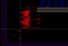
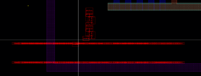
Initially extracted RC and mosfet symbols without any problem like in Image #1, but did something wrong in the settings and now symbols are not being extracted like in Image #2...

No idea what happened :S

Could you guys help me out with how to fix this..? Any help would be much much appreciated... :(

Thank you so much in advance..

<Image #1>
1.png

<Image #2>
2.png
 

The images has too low resolution to see what's going on but two things might have happened.

1. You changed the extraction view settings which show up after the extraction is done. Here you can select arrayed placement or as in schematic, not sure about what it is called exactly.

2. You disabled parasitic extraction. In the output tab you can select between r, c, c+cc etc. See what you have there.
--- Updated ---

Something went wrong the first time I opened the images. Now I can see them more clearly. I bet option 2, you have turned off parasitic extraction, is your problem.
 

Hi martinnl, thank you for your response. I enabled parasitic extraction and set the outputs in the output tab as you mentioned, but it did not work...

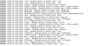
It keeps showing 'Warning: Could not find layers...' as the picture below.. Do you know what's causing this problem..? Any type of support would be greatly appreciated..

3.png
 

It could be that the layer map is incorrect. It think it is defined under the input tab or the rules tab.

Calibre creates a GDS file in the run directory. If it's in ASCII format you can open it and look at which layers it contains and see if it is correct. Otherwise stream it in and take a look. It's probably a good idea to do this on a sample layout with perhaps a single metal rectangle or a single transistor, the minimum you need to see the error.
 

Status
Not open for further replies.

Part and Inventory Search

Welcome to EDABoard.com

Sponsor

Back
Top