Continue to Site

Welcome to EDAboard.com

Welcome to our site! EDAboard.com is an international Electronics Discussion Forum focused on EDA software, circuits, schematics, books, theory, papers, asic, pld, 8051, DSP, Network, RF, Analog Design, PCB, Service Manuals... and a whole lot more! To participate you need to register. Registration is free. Click here to register now.

Cadence Inverter using verilog

Status
Not open for further replies.

kimo4ever

Member level 2
Joined
Dec 10, 2010
Messages
45
Helped
0
Reputation
0
Reaction score
0
Trophy points
1,286
Activity points
1,574
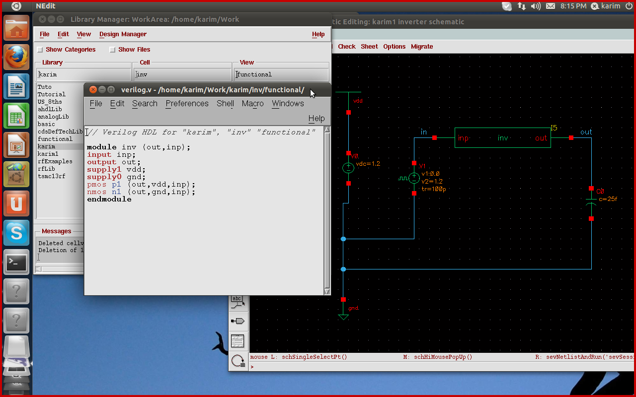
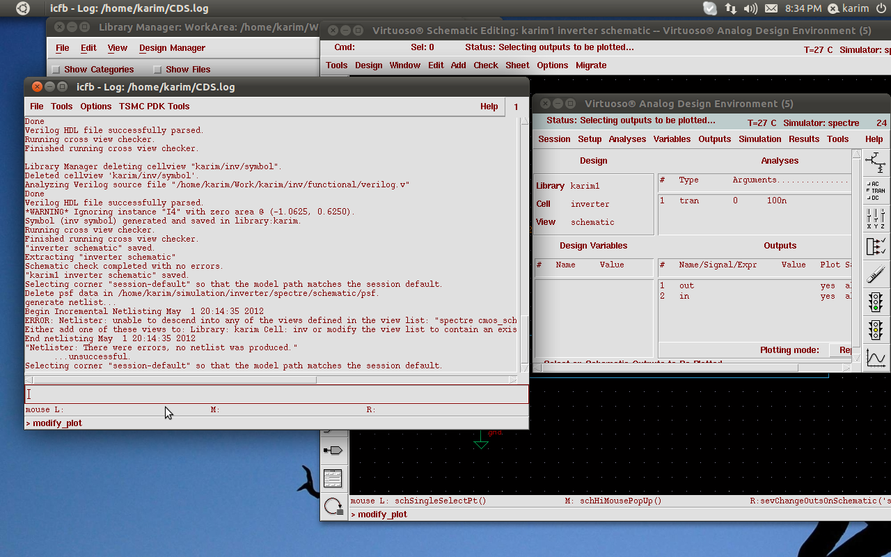
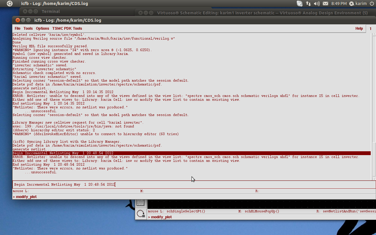
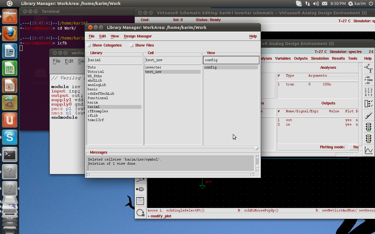
I am new in cadence, and i am trying to learn how to use the verilog to create my cct, so i learnt how to type my verilog code, in a functional view, but my question ,
1) what are the steps to do for example an inverter using verilog?
2) have i to do its schematic first then from schematic to symbol then functional where i type my verilog, ? or i can generate from my functional file the symbol and the schematic ?
thnx
 

1) Write code for inverter. Save it and correct any errors. Generate symbol for that code. When you close the verilog file and there are no errors then cadence will ask you if you want to create symbol click yes and it will automatically generate symbol. Once the symbol is created you can test it.

2)I don't think you can generate schematic from functional file (I am assuming by functional you mean VerilogA code ?) or functional file from schematic (perhaps others can shed some light if there is some software for this) But you can generate a symbol from a schematic.
 
thnx for the reply, actually, i use verilog editor, for digital circuits, not verilog A, but it is ok, i did these steps, until i found in a tutorial that we do a schematic then the functional, however,i will search in how to test a symbol, actually i am in this step now, and if you can help me, or give me some tutorials i would be very thankful
Thnx again :)
 

you are welcome :). Once you have a symbol, you can place it in your schematic file like any other part that you would place. Open a new schematic file. Open the place component menu...it can be opened by pressing "i". Find your symbol in that list and place it in the schematic. Now your symbol will have some inputs and outputs. Just connect those to your test signals. and see the output waveform.
 
okok, after i created my symbol, after the verilog , i opened a new schematic as you told me, then wired all the necessary components (Vdd ,Vdc,gnd and a cap and Vpulse) then i check and save , without errors, then i chose tools-->analog environment then i labled the wire and set them to be simulated , but it told me there is an error, and don;t wanna to simulate, is that coz of my simulation method?
 

What does the error say? Your simulation method seems ok.
 

after setting the simulation paramters as transit and sepcifie the out and inp nodes, i press netlist and run and that error appear in the CIW:
Netlister:there were errors , no netlist was produced
....unsuccefull
knowing that after i click save and check after the schematic, it says that no errors occurs

Open your verilog file and then based on the text editor you are using close the file again...cadence will give a message that the file has been successfully compiled or not. If it say failed then there are some error inside your verilog code.....I do this for Verilog A perhaps verilog is also the same
 
yes, my verilog code after existing it says it was sucessfully compiled, so there no error in code, here a screen shot of my work, knowing that,m the schematic and the functional are not in the same library as i understood from you
 

this schematic and the Inv code are in different libraries..but that shouldnt be a problem...The verilog code that your are using, I am not familiar with it. Can you also post a screen shot of the log that displays when you netlist and run this ?
 

okok, the simulation analysis is :transient i also pick a screen shot of its window, and you can find what it says to me when i run it at the last three sentences in the CIW
 

Can you expand the window because I want to read the line i think 4th from Bottom which starts with ERROR . also if possible a screenchot of your library manager showing where your inverter is and where the testbench for inverter is
 

the verilog functional file and the symbol is in library called :karim ....and the schematic is in the library called: karim1
 

I am out of ideas but dont you have to include some libraries in your verilog code to use the pmos and noms reserved words? Also in the test_inv config....infornt of the Inverter name is the verilog view selected? I mean if inverter is in VerilogA then verilogA view needs to be selected in config of test_inv. similarly for other verilog versions
 

mmm, i don't know actually, using these keywords was a option, i begin by using a simple verilog code at gate level using ( not (out,inp) , and same problem , so i used the transistor level , but nothing at all, i will check the verilog editor ( mine in called nedit) and check the verilog libraries and see what was the issue,
thnx for your help so much :) and i will write to you when i got the problem with the solution :)
 

Yes I am also curious to know what could the problem be....did you check the setting insde the config for test_inv?
 

Sorry, yesterday, i didn't catch your reply, but actually, i don't wanna say that the config file creation didn't completed correctly coz of a missing file in my cadence:D:D, i will try to connect my TA in this grad project these days, to modifie my cadence version or something, and i will update you with the news :)
 

Status
Not open for further replies.

Similar threads

Part and Inventory Search

Welcome to EDABoard.com

Sponsor

Back
Top