Continue to Site

Welcome to EDAboard.com

Welcome to our site! EDAboard.com is an international Electronics Discussion Forum focused on EDA software, circuits, schematics, books, theory, papers, asic, pld, 8051, DSP, Network, RF, Analog Design, PCB, Service Manuals... and a whole lot more! To participate you need to register. Registration is free. Click here to register now.

Buffer driving capability

Status
Not open for further replies.

Junus2012

Advanced Member level 5
Joined
Jan 9, 2012
Messages
1,552
Helped
47
Reputation
98
Reaction score
53
Trophy points
1,328
Location
Italy
Activity points
15,235
Hello,

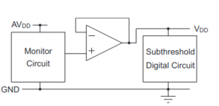
I am using the buffer like the picture shown below. The unity gain buffer amplifier is buffering the input voltage and use it as the supply voltage source for the coming digital cell.
It very known that for the digital cmos gates, the supply current and is proportional to the frequency of operation and the digital cells consumes the highest current in the transition region.
So what is happening here is that the buffered opamp need to supply this current otherwise the buffer output will drop.

What is possible solution to improve the current driving capability of the buffer ?
Do we need a low output opamp, or even OTA can serve in this purpose?

Thank you
Regards
 

Attachments

  • buffer.png
    buffer.png
    9 KB · Views: 159

Basically, you need a very low output impedance driver for the supply at your digital logic frequency of operation. You can either design a very high bandwidth opamp loop to have low impedance at fo or you can add a big fat cap at the output of the opamp which supplies the switching current drawn by the digital blocks. In the second case, your opamp loop bandwidth should be enough to replenish the charge lost by the fat cap to certain level in every clock cycle.
 
This is a classic LDO scenario. Amplifier can not respond fast enough to sharp increases in the load current caused by digital circuits switching. So, a big cap at the output is taking care of the instantaneous current jumps until the amplifier wakes up and takes over.
 
If you're going to do a LDO design and you have the
headroom, use a NMOS source follower pass FET; it
can surge current a lot quicker than a PMOS pass FET
which acts quasi-contant-current on load-step. The
NMOS will act quasi-constant voltage (a much lesser
voltage excursion prior to loop re-closing).
True. But a NMOS pass FET gives a poorer PSRR.
 

Maybe I will learn something here. I thought NMOS has higher mobility than PMOS.
So in a control loop there is more G for PSRR enhancement than PMOS in the loop ?

Regards, Dana.
 

    Junus2012

    Points: 2
    Helpful Answer Positive Rating
Dear friends

Thank you for your useful discussion,

I understood from you the necessity of using the LDO (in case I have enough voltage headroom),
but what about a more simpler solution by using the VI converter as shown below, where R represent my digital circuits.

Thank you
Best Regards

regulator1.png
 

"Normally" you dont drive your digital circuits with a current source,
so not sure why you are suggesting this ?


Regards, Dana.
 

    Junus2012

    Points: 2
    Helpful Answer Positive Rating
"Normally" you dont drive your digital circuits with a current source,
so not sure why you are suggesting this ?
Thanks Dana,

Because I saw this transaction on IEEE "Analysis and Design of an Ultralow-Power CMOS Relaxation Oscillator",

please see the picture below to see how he used the buffer like VI converter to supply the digital circuit with VDIG voltage

regulator2.png
 

Hi,

I agree with danadakk.
in post#1 you say that it should supply a "digital cell".

It seems your requirements have changed...

Klaus
 

Hi,

I agree with danadakk.
in post#1 you say that it should supply a "digital cell".

It seems your requirements have changed...

Klaus
Hi klaus,

not changed, if you see my last post still I am talking about VDIG for supplying digital circuit, and by the way you can consider the relaxiation oscillator as an example of digital load.. same concept :)
 

True. But a NMOS pass FET gives a poorer PSRR.
Not necessarily. A PMOS FET with comp cap wrapped
D to G can amplify (not just fail to attenuate) supply
ripple. A NMOS pass FET requires the gain to be had
elsewhere (P pass FET contributes a significant gain
but that's also quite variable w/ load-point, headroom
and so on, making "quick and dirty" loop compensation
a trap).

DC PSRR is one thing. HF PSRR is another and some
designers may not pay attention to this application
"care-about" which doesn't always (in the past, never)
show on datasheet electrical tables. Yet HF PSRR is
what point of load LDOs are supposed to fix, in a lot
of design-ins.
If you are compensating the loop with a huge cap at the output node, you are already expected to get decent/good HF PSRR. However, in this process, using an NMOS pass FET makes it difficult to make the output pole the dominant one, because of the 1/gm kind of output impedance looking back from output node in open loop configuration (more so as gm of the pass FET will be relatively very high since it carries the supply current for the load it is driving). Also, the headroom may not work out well for the previous OTA stage, as NMOS Vgs needs to fit in now. Furthermore, the DC PSRR is always expected to be better with PMOS pass FET, for the same total DC power consumed including the OTA power ( mainly because the NMOS source follower stage doesn't provide any DC gain).

I would argue that a PMOS pass FET is a natural choice bacause of its ease of implementation in almost all cases. However, an NMOS pass FET achieves a lower output impedance over a wider bandwidth, but cannot outperform a big fat cap in these applications that we are talking about.
 
Thank you dear friends for your help,

you made it clear for me, and I am going to summarize it for you.

If I am supplying digital cells with a low dynamic current that a buffer amplifier can handle, then I simply will go for it.

if the load consume high power (especially the dynamic power ) that drop the output of the buffer amplifier, then a simple modification has to be done by using NMOS or PMOS in the loop of the buffer to supply pass the current from the supply voltage, not from the opamp buffer itself, which then we call it low drop output voltage regulator. In the latter form the output voltage will be regulated against the load variation. The NMOS or the PMOS used must keep enough voltage headrom for the load circuit.

Thank you once again
Regards
 

Status
Not open for further replies.

Part and Inventory Search

Welcome to EDABoard.com

Sponsor

Back
Top