Continue to Site

Welcome to EDAboard.com

Welcome to our site! EDAboard.com is an international Electronics Discussion Forum focused on EDA software, circuits, schematics, books, theory, papers, asic, pld, 8051, DSP, Network, RF, Analog Design, PCB, Service Manuals... and a whole lot more! To participate you need to register. Registration is free. Click here to register now.

Buck converter Error Amplifier Circuit Parameters, need an urgent help

Status
Not open for further replies.
Your small signal compensation looks okay, I'm seeing a crossover frequency of about 80KHz with a phase margin of about 50 degrees. It should be stable (in the small signal sense).
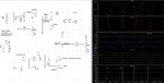
Can you please show me on the output graph how do you see crossover freq 80kHz? I am measuring the output of the error amplifier to see crossover freq and phase margin. Is it wrong?

Looking at the transient simulation, it looks like there are many problems with the PWM modulation. Like crutschow pointed out you don't have any ramp signal, which means things simple won't work. Also your switching frequency needs to be at least twice your crossover frequency, in practical terms a factor of five is more reasonable. Also I doubt your gate drive circuit will work effectively at 150KHz, it's probably too slow.

Yes, both of you are right. I actually replaced my pulse with the sawtooth and i will do it in the board as well. I will try to use pwm driver. Can you suggest me any driver?

thanks a lot!

- - - Updated - - -

You're correct about R2 of course. I didn't look carefully at the schematic and thought it went to ground, not the MOSFET gate. :oops:

You don't seem to have enough output capacitance to give a reasonable low ripple voltage. I got a reasonably stable output by changing C1 to 20µF, reducing the loop gain by changing R5 to 42kΩ, and rolling off the loop response by changing C4 to 1nF (Those are not optimum values since there is still some low-level oscillation in the inductor current). The output ripple was about 20mVpp with those values.

I used a soft-start time-constant of 0.6ms, which avoids any significant start-up overshoot.

Note that you should have a resistor in series with Q1's collector since there's noting to limit the current through the zener diode D2 when Q1 is ON. Something between 500Ω and 1kΩ should work.

gotchaa! Now it looked much better! Btw, Soft start time mean RC time constant right?
 

...............


gotchaa! Now it looked much better! Btw, Soft start time mean RC time constant right?
Yes, it's the time-constant of the Vref output.

Edit: Don't know of any other PWM modulators designs off hand. Using a sawtooth (or triangle) ramp is the common way to do it.
 
Last edited:
Yes, it's the time-constant of the Vref output.

Edit: Don't know of any other PWM modulators designs off hand. Using a sawtooth (or triangle) ramp is the common way to do it.

Thnx a lot for your help! that was really helpful!
I have one more question. I wanna try synchronous buck converter by replacing the freewheeling diode with the pmos but i could not realized how to model mosfet driving seperately. Because i am only having one output from the comperator (PWM modulator) and i could not realize how to feed two mosfet with only one output that i have from the modulator :) Can you please help me ?
 

I have one more question. I wanna try synchronous buck converter by replacing the freewheeling diode with the pmos but i could not realized how to model mosfet driving seperately. Because i am only having one output from the comperator (PWM modulator) and i could not realize how to feed two mosfet with only one output that i have from the modulator :) Can you please help me ?
A synchronous MOSFET diode is turned on with the opposite phase to the switching MOSFET. The trick is to adjust the two signals so there no significant overlap between the two transistors, since if they are on at the same time, it's a short circuit from the input power to ground.

If you use an N-MOSFET for the diode than the signal for the P-MOSFET series switch and the N-MOSFET diode have the same polarity. An N-MOSFET will work for this since a MOSFET will conduct in either direction when ON.

As I understand, i will use p-MOS for the high side and n-MOS for the Low side and both MOS will be feed from the same pwm since they have the opposite polarity? I have built that schematic and try to observe transient response of that and results seems to be ok for me. what do you think for the schematic and results? Thanks a lot for your help ! SynchTransient.jpgforum sync schematic.jpg
 

As I understand, i will use p-MOS for the high side and n-MOS for the Low side and both MOS will be feed from the same pwm since they have the opposite polarity? I have built that schematic and try to observe transient response of that and results seems to be ok for me. what do you think for the schematic and results?
That won't work. Because of the signal inversion caused by Q1, both transistors turn on together, which shorts the input to ground. You need an inverter added to one of the signals.
 

Hi again,

I have used an inverter in the circuit as you said. Output voltage looks perfect! But As i see from the fig attached, M1 is not switching ON correctly. I tried to increase Rgshigh to increase tau but it did not work. Why do you think i am having error in the circut? what would you advise to me?
Thanks a lot in advance!
 

Attachments

  • forum.jpg
    forum.jpg
    463.4 KB · Views: 73

But As i see from the fig attached, M1 is not switching ON correctly. I tried to increase Rgshigh to increase tau but it did not work. Why do you think i am having error in the circut? what would you advise to me?
Thanks a lot in advance!

I believe R3 (500 ohms) should be a lower value, to draw M1 gate down to a lower volt level.
 

Status
Not open for further replies.

Similar threads

Part and Inventory Search

Welcome to EDABoard.com

Sponsor

Back
Top