Continue to Site

Welcome to EDAboard.com

Welcome to our site! EDAboard.com is an international Electronics Discussion Forum focused on EDA software, circuits, schematics, books, theory, papers, asic, pld, 8051, DSP, Network, RF, Analog Design, PCB, Service Manuals... and a whole lot more! To participate you need to register. Registration is free. Click here to register now.

Bootstrap doesn't work

Status
Not open for further replies.

VTI_16V

Member level 1
Joined
Nov 25, 2019
Messages
38
Helped
0
Reputation
0
Reaction score
0
Trophy points
6
Activity points
386
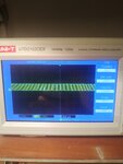
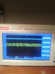
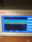
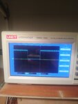
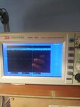
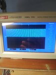
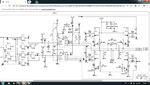
Hello. I am struggling with this for whole day and i just can't figure out what is wrong. I had similar problems, but nothing like this. So i have 2 IR2183 which are used for h- bridge. As I can see on the scope the logic side before IR2183 is fine. I am receiving good signals on pins 1 and 2 on both of them. But on pins 7 i have this (picture with pwm that doesn't look like it should), and on the other hand here is a picture of pins 4 of IR2183 which are turning on low side mosfets which seems fine to me? R39 resistor was burnt, i changed it. D32 is tested fine, D1 is also tested fine. I changed IR2183, still same, the old ones are also working fine on the other device. IRFZ mosfets are also tested ok, diodes D2, D3, D4 also OK, capacitors C1, C2, C4,5,6 and 7 are not blown neither shorted, so I assume they are also fine. No signs of any corrosion on PCB or broken tracks. No signs of any short when i pull off the final mosfets. When they are in the PCB i get short on final mosfets because the bootstrap doesn't work This is driving me crazy, i don't know what to look for anymore. You can ask whaever you want, i will take a measure and post it here, i would be thankfull because i really want to solve this problem, i have a feeling that it is something stupit in front of me what i don't see.
 

Attachments

  • IMG_20200902_123233.jpg
    IMG_20200902_123233.jpg
    4 MB · Views: 126
  • IMG_20200902_123513.jpg
    IMG_20200902_123513.jpg
    4.4 MB · Views: 138
  • schema.png
    schema.png
    160.9 KB · Views: 149

Hi,

What´s the use of C4..C7?

I don´t like the undamped LC combination at IRxxxx supply. It causes a resonance maybe with huge oscillations.
In either case C18 and C17 are too small (value). They need to provide the complete swtich ON current of the low side Mosfets.
I´d connect 10uF at least in parallel.

Node D1_Anode needs to have a capacitor. It needs to provide the complete swtich ON current of the bootstrap circuit. (high current pulses)

What´s your HD_PWR voltage?

Did you design a suitable PCB layout with solid GND plane and low impedance pulse paths?

Klaus
 

I didn't design this, this is autopilot computer from manufacturer raymarine. HD_pwr voltage is around 12V
--- Updated ---

I dont doubt in your knowledge friend, but mistakes that are made in production won't help me because there are large number of theese computers on the boats and they are working for a long time, i would like to stick to this specific problem so I can try to solve it... If you have some idea, i would appreciate it :)
 
Last edited:

Hi,

I was mistaken: I thought it´s your new design...

So let´s try to find what´s wrong:
* disconnect R3
* disconnect R12
(now the HIGH side is decativated)
power up the device. everything should be cool, current consumption some 10 of mA.
There should be PWM on the driver inputs.

Focus on TR6:
* Measure the voltage of these pins with a DVM and tell us: 3, 4, 5, 6
* show a two ch scope picture of pin 1 and pin 2
* show a two ch scope picture of pin 2 and pin 4
* show a two ch scope picture of pin 1 and pin 7

if you think every thing is fine, then do the same with TR7.

Klaus
 

    VTI_16V

    Points: 2
    Helpful Answer Positive Rating
Here goes. First picture is on pins 1&2, second is 1 & 7 and third and forth are 2 & 4. Don't let forth picture confuse you, it is in mode when reverse direction is applied. All other pictures are when trying forward direction. On pin 3 I have 0V, on pin 4 11.2 when in reverse direction, and 8.5 when in forward direction (when PWM starts). On pin 5 12.6V and pin 6 11.6V. I got the same reading on pins 6 and 7, and i am reading same pwm on pin 6 like in the picture on pin 7...
 

Attachments

  • 1 I 2.jpg
    1 I 2.jpg
    1 MB · Views: 98
  • 1 I 7.jpg
    1 I 7.jpg
    1.1 MB · Views: 97
  • 2 i 4 (2).jpg
    2 i 4 (2).jpg
    1.3 MB · Views: 97
  • 2 i 4.jpg
    2 i 4.jpg
    1.1 MB · Views: 86

Hi,

Please confirm: did you disconnect R3 and R12 before the measurements?

Klaus
 

Assuming If HD PWR =12V with Vboost node only going from 12V to 17.5V, so P66 appears to be loading the output from Pin 6 thru C2 clamped by D1B. The TP66 load ought to be 150uA or ~6KOhm. This is just a negative clamp circuit so the Vs signal should be positive rectified on VB above HDPWR.
 

I contiued... I took of R6 and R9, and now on the pins 7 I don't get any pwm, it just stands on 12V althought the signals on inputs seems ok... Anybody got some idea? Edit: i'm still a noob, but if i figured out right, there shouldn't be any output on pins 7 with low side mosfets turned off? This is confusing me... So when motor starts to go in one direction, TR2 should be turned on and off by pwm... In on position it is connecting the ground to pin 6 so capacitor C2 should be charged for bootstrap. So next what should happen is, when TR2 turns off, pin 6 on TR7 should be floating or connected pin 6 internally somehow so that capacitor stays charged and then discharged internally over the pin 8 of TR7 and then through pin 7 of TR7 so it can turn on high side TR1? Am I right? So what counfuses me that in all that time TR3 is turned ON for ground connection and when motor is not present(disconected), it supplies ground all the time when is turned on through R15? So, how can pin 6 be floating or internally connected to + when there is always ground through R15? I would really like to solve this, but I am out of ideas :(
--- Updated ---

I managed to get a hold of a similar unit that works. So i was not mistaken, the input signals on the gates of low level mosfets, i should see the same signal switching on the drains of low side mosfets. But I don't see anything switching, it just remains ground which means that boot capacitor won't charge/discharge. But all the low side mosfets are tested OK and both tr7 and tr6 are NEW.
 
Last edited:

Hi,

The bootstrap circuit has nothing to do with low side signals. It's for high side only.

Klaus

Added:
Scope picture: please show just about 5 pulses per screen. With 100 pulse we can't see any details.
And please don't make one channel overwrite the other. Change Y positions.

With a 5V input pulse you should see 12V output pulses for the low sides.

Klaus
 
Last edited:

Hello, i wanted to say that bootstrap won't work if the low side mosfets are not turning on... Maybe I am mistaken but aren't low side mosfets TR2 and tr3 thoose which should connect grounds to bootstrap capacitors? The problem is that TR2 and TR3 are not oscillating although they are receiving pwm on gates from pins 4 of tr6 and tr7... I compared input signals from TR 6 and 7 with the device that is working fine and they are the same. The output from tr 6 and 7 on the pins 7 can not produce bootstraped voltage when transistors tr2 and tr3 are not switching and they are not switching AT ALL altghough they are fine, i tried with other mosfets, same thing happens...
 

Hi,

Correct.
But first things first.

5V driver input --> 12V driver output (low side) --> 12V Mosfet gate --> 0V Mosfet drain --> 0V driver VS input.
(This should be true for pulsed signals as well as continuous (DC) signals)

Verify this chain, step by step.
You may additionally check:
* Mosfet type, datasheet, pinning
* Mosfet source signals.
Please check the voltages directly at the pins of each device. Just to be sure there are no soldering problems..

Klaus
 

You make this sound like a 'fix it, but don't change anything'. Is this a repair or a new design? Did it ever work? Is it power supply or motor controller.

Best if you hook up scope with differential add probes across boost caps. 1 uF boost caps sounds like overkill in size for supplying just highside gate drive

If input driving signals are not phase timed correctly it could impact boost cap charging cycle.
 

Status
Not open for further replies.

Part and Inventory Search

Welcome to EDABoard.com

Sponsor

Back
Top