Continue to Site

Welcome to EDAboard.com

Welcome to our site! EDAboard.com is an international Electronics Discussion Forum focused on EDA software, circuits, schematics, books, theory, papers, asic, pld, 8051, DSP, Network, RF, Analog Design, PCB, Service Manuals... and a whole lot more! To participate you need to register. Registration is free. Click here to register now.

[SOLVED] Board review request (frequency converter)

Status
Not open for further replies.

m4rtinpf

Newbie
Joined
Jun 30, 2021
Messages
5
Helped
0
Reputation
0
Reaction score
0
Trophy points
1
Activity points
46
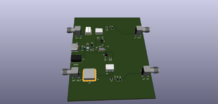
I've designed a PCB and was looking for some review and advice. The images are attached to this post.

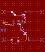
The board is for an up/down frequency converter. Specifically, from 0-300 kHz to 400 MHz.

It's a simple design, the input signal gets multiplied by a 400 MHz square-wave (X1) by a mixer (U6 or U2). There are also two LPF and limiters.

Power comes from a USB connector or a terminal block and gets regulated down to 3.3 V by U5.

I'm planning to get it fabricated by JLCPCB, including the assembly of the SMT parts that they carry. I would have to hand-solder the ICs (or get someone to it). It's a two-layer board, and I need a single unit.

The size of the board is due to the enclosure I'm gonna use (Hammond 1455L801).

I have a few questions:

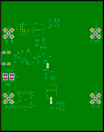
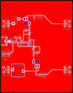
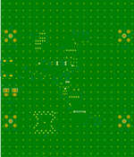
1. The ground plane is split in two places:
- The (amplified) clock signal (400 MHz square-wave) from U4 to C3, so VCC can get to the other side of this trace.
- The down-converted signal (<300 kHz) from U6 to L2, so this trace and the input signal (400 MHz) can cross.

Is this OK or using 0R resistors would be better?

2. Should I remove the solder paste from the ICs that I'm not getting soldered by JLCPCB?
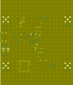
3. Are the vias connecting the top-layer filled zones to the ground plane enough and well placed (besides the ones under the ICs, just followed the datasheets for those)?

Thanks in advance for any help!

PS: There is a minor misalignment between layers in the images. It's because of a bug in Kicad that makes it so silkscreen is under copper when plotting to PDF, so I had to manually stack the individual layers.
 

Attachments

  • converter_3d.png
    converter_3d.png
    58.1 KB · Views: 183
  • converter_bom.png
    converter_bom.png
    96.7 KB · Views: 195
  • converter_pcb_bottom.png
    converter_pcb_bottom.png
    385.4 KB · Views: 240
  • converter_pcb_top.png
    converter_pcb_top.png
    468.9 KB · Views: 187
  • converter_schematic.png
    converter_schematic.png
    450.3 KB · Views: 251

Hi,

I´m no HF guy.
But for my taste the power supply capacitors of U3 and U4 are too far from pad#1.
Did not look deeply through the HF circuit..

***
You use ath aluminum case. You move the PCB inot the slots.
* if you want the aluminum case isolated from the PCB_GND planes then remove the copper at the slots.
* but if you want the aluminum to be connected to the GND planes, you could remove the solder stop. Because of the anodisation (not good conductive) you still won´t get a reliable connection. But if you remove the anodisation you could improve....

Klaus
 

    m4rtinpf

    Points: 2
    Helpful Answer Positive Rating
Hi,

I´m no HF guy.
But for my taste the power supply capacitors of U3 and U4 are too far from pad#1.
Did not look deeply through the HF circuit..
The capacitors are around 60 mil (1.5 mm) vertical and 40 mil (1 mm) horizontal apart and JLCPCB recommends at least 40 mil between 0402 and QFN components.
As for the layout, I based it on the one in the datasheet (see attached).

Did I do something wrong? I guess I could move them so they are 40 mil vertical apart too...

And I just realised that the NC pins can be tied to GND.

***
You use ath aluminum case. You move the PCB inot the slots.
* if you want the aluminum case isolated from the PCB_GND planes then remove the copper at the slots.
* but if you want the aluminum to be connected to the GND planes, you could remove the solder stop. Because of the anodisation (not good conductive) you still won´t get a reliable connection. But if you remove the anodisation you could improve....

Klaus
I'll remove the copper from the piece of board that goes into the slots then. Thought that the silkscreen would be insulation enough, but that would not be so after it gets scratched.
I want the enclosure to be connected to GND only on the coax connectors (with a nut and serrated washer) so as to not get ground loops.

Thanks!

Edit:
I've noticed that some ICs (the ones that I made the footprints for, X1 U3 U4 U7 Q1 U5) have thermal relief ("spokes"), but the rest don't. Should I add it to all of them? Remove it?
 

Attachments

  • Screenshot_20210630_160121.png
    Screenshot_20210630_160121.png
    75.8 KB · Views: 181
Last edited:

The capacitors are around 60 mil (1.5 mm) vertical and 40 mil (1 mm) horizontal apart and JLCPCB recommends at least 40 mil between 0402 and QFN components.
Are you sure you are talking about pin1?
There is no scale, but I think the trace length from pin1 to capacitor is rather 15mm...

Thermals:
I'm quite sure that a member with HF experience will tell you to remove the thermals --> lowest inductance connection to the copper plane.

Did you care about trace impedance?

Klaus
 

Are you sure you are talking about pin1?
There is no scale, but I think the trace length from pin1 to capacitor is rather 15mm...
Sorry I was talking about clearance. Yes, trace length is about 15 mm.
Thermals:
I'm quite sure that a member with HF experience will tell you to remove the thermals --> lowest inductance connection to the copper plane.
As long as the lack of them won't bring much trouble while soldering, I'm up for removing them then.
Did you care about trace impedance?

Klaus
I did not.
The oscillator generates an LVDS square wave, so the rise time is at least 200 ps.
So the TEL (Transition Electrical Length) is about 28 mm. The longest trace between the oscillator and the mixers is around 9 mm, so I didn't consider it necessary, but maybe it's easier to just change the trace width so they are 50 ohm...


TEL=trc0√ϵr=200[ps]3×10⁸[m/s]√4.5=28[mm]TEL=trc0ϵr=200[ps]3×108[m/s]4.5=28[mm]​


"Calculating TEL for a given rise time is a method for obtaining a first order estimate of whether or not a design is fast enough to require the use of transmission line management rules. If a design has lines as long as a TEL for that logic family, the designer can be assured that the design will require careful management of impedance in order to avoid reflection problems."

Lee W. Ritchey. Right the First Time: A Practical Handbook on High-speed PCB and System Design. Speeding Edge, 2003. isbn: 0974193607,9780974193601.

Edit: Just checked and the traces would have to be 2 mm wide for 50 ohm. That's wide enough to short the IC pads, so can't do it.
--- Updated ---

Looked around around and controlled impedance isn't necessary if trace length<electrical length/10 (or /6 maybe). So I can:

* Make the clock traces <2.9 mm
* Filter the square wave to get slower edges
* Switch to a 4 layer board

Not sure what's the best choice
 
Last edited:

Thermals:
Should be no problem with reflow soldering.

Trace impedance.
It will work without impedance matching.
I think I'd just use 2mm wide traces where possible...at least at the lengthy traces. From the pads use narrow traces as you like, then - where possible - use 2mm.

I don't see it very critical. If done correctly you need
* 50 Ohms source impedance
* 50 Ohms traces
* 50 Ohms termination
I'm not sure if it's worth the effort.

An experienced member should comment on this.

Klaus
 

    m4rtinpf

    Points: 2
    Helpful Answer Positive Rating
I ended up going for a four-layer design.

The stackup is:

- Layer 1 (F_Cu): Signal 1
- Layer 2 (In1_Cu): GND
- Layer 3 (In2_Cu): Power
- Layer 4 (B_Cu): Signal 2

I used the 7628 prepreg from JLC PCB (https://cart.jlcpcb.com/impedance).

Layers 2 and 3 are uninterrupted, layer 4 is all ground except for a single trace.

*Note:* JLC PCB only does through-hole vias.

Is it okay to only route one trace on layer 4 (I feel like I'm wasting it lol)?

I thought about the possibility of switching to stripline, but all signal traces would have to go to layer 2 through vias. And I don't know if it would even be useful.

Do I need to add RF shielding between the different parts of the circuit (like FR4 "walls" or proper cans)?

Thanks for all the help!
 

Attachments

  • converter-B_Cu.png
    converter-B_Cu.png
    117.3 KB · Views: 166
  • converter-F_Cu.png
    converter-F_Cu.png
    158.5 KB · Views: 165
  • converter-In1_Cu.png
    converter-In1_Cu.png
    112.8 KB · Views: 181
  • converter-In2_Cu.png
    converter-In2_Cu.png
    217 KB · Views: 175

Hi,

there are many ways .. not the one and only one.

It may be a waste of layers and money.

For sure it can be done on a 2 layer board. But if you want a 1.5mm thick board then there are the 2mm wide 50 Ohms traces. Not very nice.

Ask three engineers and get three different opinions.
Good thing: there is no "wrong". So do it now as a 4 layer board. Find out the drawbacks and benefits and gain experience. With this experience you may decide next time on your own which way to go.

For a single unit you won´t become poor. Producing a million pieces is a different story.

Klaus
 

    m4rtinpf

    Points: 2
    Helpful Answer Positive Rating
Update:

Last week I was finally able to test the board and it works!

Picture here:

IMG_20210818_111607_1.jpg

The board was done by JLCPCB, who also soldered the passives.
A local shop soldered the ICs (hence the melted U4 on the top left).

Just posted back to say thanks for all the help!
 

Hi.

Well done.
Still I recommend to do some HF PCB layout tutorials. Especially regarding via placement.

Klaus
 

Status
Not open for further replies.

Part and Inventory Search

Welcome to EDABoard.com

Sponsor

Back
Top