Continue to Site

Welcome to EDAboard.com

Welcome to our site! EDAboard.com is an international Electronics Discussion Forum focused on EDA software, circuits, schematics, books, theory, papers, asic, pld, 8051, DSP, Network, RF, Analog Design, PCB, Service Manuals... and a whole lot more! To participate you need to register. Registration is free. Click here to register now.

BJT question_2

Status
Not open for further replies.

khatus

Member level 3
Joined
Oct 7, 2017
Messages
56
Helped
1
Reputation
2
Reaction score
0
Trophy points
6
Activity points
441
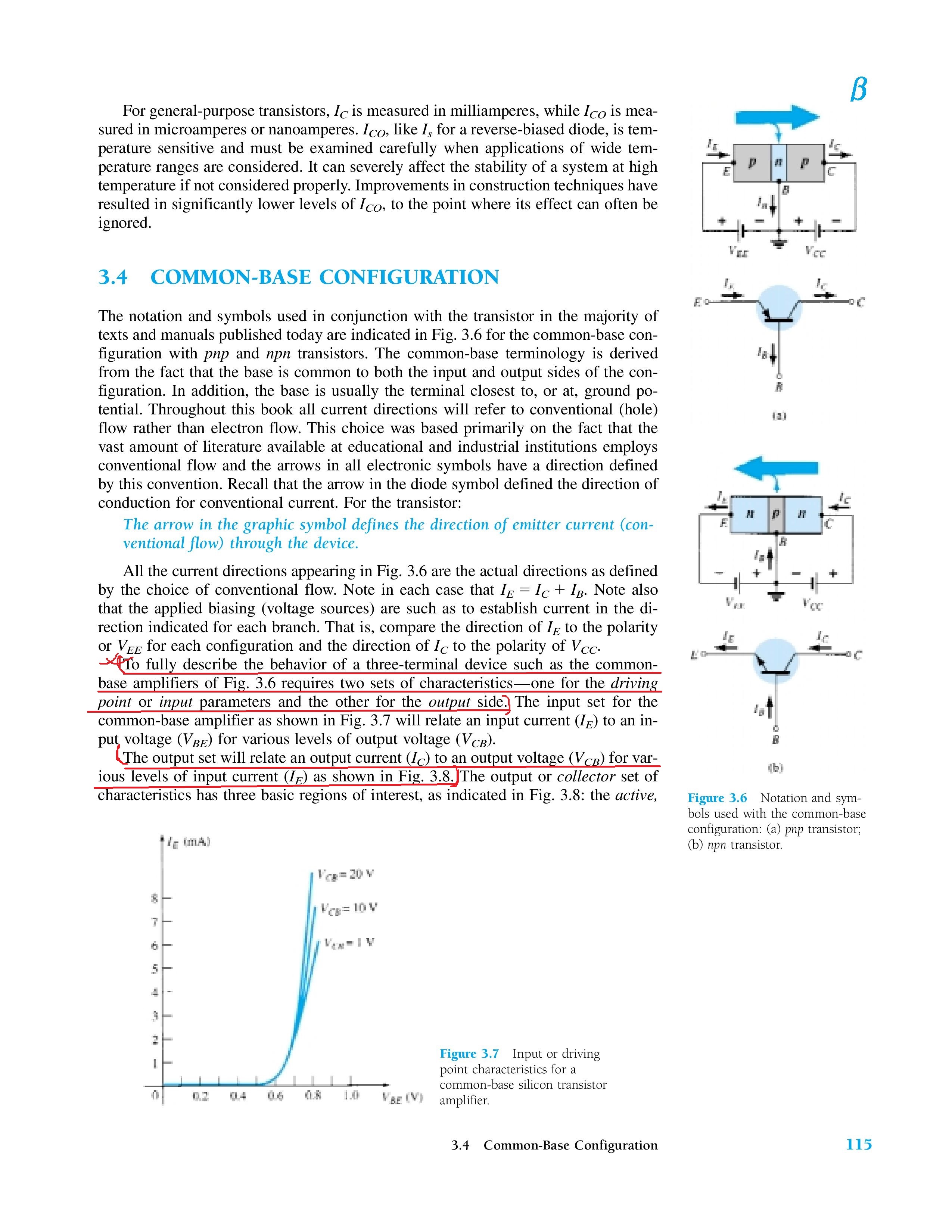
From the book Electronic Devices and Circuit Theory by Robert Boylestad, I can not understand few lines.

Electronic Devices and Circuit Theory-page-126 - Copy - Copy.jpg


Q1) Here, to fully understand common base amplifiers why we required two sets of characteristics instead of only one? what is the importance of the second characteristic?

Electronic Devices and Circuit Theory-page-126 - Copy.jpg


Q2) Why out put set consider Output current(Ic) to an output voltage(VCB) for various levels of input currents(IE)? What is the problem if I wanted to considerOutput current(Ic) to an output voltage(VCB) for various levels of input voltage(VBE?
Electronic Devices and Circuit Theory-page-126.jpg
 
Last edited:

why we required two sets of characteristics instead of only one?
I don't really understand your problem.
Since the input and output are isolated (although the input affects the output) you need one set of characteristics for the input and one for the output.
You cannot definitively determine the output voltage for a given input without knowing both characteristics.
You are welcome to try, if you think you can.
 

Why out put set consider Output current(Ic) to an output voltage(VCB) for various levels of input currents(IE)? What is the problem if I wanted to considerOutput current(Ic) to an output voltage(VCB) for various levels of input voltage(VBE?
Have a look on the hybrid equivalent model of BJT transistors on the Common Base configuration and you will realise that both VCB and IE are took into account to determine IC
 

Common-base operation works via changing emitter voltage.

Bias current merges with collector current. The input signal provides these with a path through itself. This arrangement is not so simple compared to common-emitter or commons-collector.

Changing any one parameter (volt levels or component values) makes it necessary to do a lot of adjusting and tweaking of other parameters, in order to locate a good operating point. Perhaps in this sense common-base mode requires simultaneous consideration of driving points and output points.

Practical example. Full gain of the transistor is available to amplify a weak input signal.

common base operation NPN weak AC signal receives hi gain.png
 

Status
Not open for further replies.

Similar threads

Part and Inventory Search

Welcome to EDABoard.com

Sponsor

Back
Top