Continue to Site

Welcome to EDAboard.com

Welcome to our site! EDAboard.com is an international Electronics Discussion Forum focused on EDA software, circuits, schematics, books, theory, papers, asic, pld, 8051, DSP, Network, RF, Analog Design, PCB, Service Manuals... and a whole lot more! To participate you need to register. Registration is free. Click here to register now.

BJT Differential Amplifier question

Status
Not open for further replies.

hamsiii

Member level 2
Joined
Apr 21, 2011
Messages
42
Helped
2
Reputation
4
Reaction score
2
Trophy points
1,288
Activity points
1,595
Hi all, I am new here and I am in need of help.
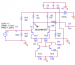
I have a project to design a BJT differential amplifier that provides a 20dB gain at the output. The circuit has a single supply (12Vdc) and the input is about 10-50mV and not differential. (Input is just a voice signal coming from the antenna)
I did some analysis but I thought they might not be correct, as output should be 100mVpp at 0Vdc. Can you help me how to DC and AC analyse this amp?
Thank you.
edit: Q3 and Q4 (with R5, R15,R16) part is for current mirror that generates 0.4-0.5mA for the diff. amp part
 

Attachments

  • reciverspice.png
    reciverspice.png
    15.2 KB · Views: 94
Last edited:

First The DC analisys and find the Q point of Q3 and Q4 very important the IC3 and Ic4, you will need it for the AC analisys.
For the DC analisys all capacitors will be replaced with a open circuit
Calculate the IC for Q3 and 4 then for Q1 ad 2.
With Ic1 and Ic2 use it to calculate the signal model for the transistor that you use.
Replace the transistors with the model and realize the calculations.

Good luck
 

i have designed the circuit properly, it gives 20dB gain but when I have implemented the circuit on a breadboard, it does not give any output. I have checked for short and open circuits, i have replaced the BJT's and check polarities of capacitors, nothing is missing and circuit is not working. Any suggestions?
 

Fault detection of BJT circuits should start with a DC bias point check. What are the dc voltages at the Q1 and Q2 collector nodes?
 

for q1 and q2: 6.1Vdc at C, 5.9vdc at B and 5.3Vdc at E.
for q3 and q4: 600mVdc at B, 0Vdc at E.
C pin of Q3 : 5.1V.
C pin of Q4 : 600mVdc.
 

0Vdc at E.

That means: No current through Q3 and Q4.
 

q3 and q4 is creating a current mirror for the actual circuit, in an example there were not any resistors at E of q3 and q4. Anyway I'll try to edit there, thanks for the answer.

edit: thanks for the reply, i set the E pins of Q3 and Q4 to 1-2vdc.
 
Last edited:

Status
Not open for further replies.

Similar threads

Part and Inventory Search

Welcome to EDABoard.com

Sponsor

Back
Top