mvj
Advanced Member level 4
Hi All,
I am using ams process and the bipolar in this has 4 teminals instead of 3. May I know what the 4th terminal is and where should it be connected.

The terminal on the top is collector
left side - base
bottom - emittor
what is the one in the middle?
Thanks a lot in advance!!
M
I am using ams process and the bipolar in this has 4 teminals instead of 3. May I know what the 4th terminal is and where should it be connected.
The terminal on the top is collector
left side - base
bottom - emittor
what is the one in the middle?
Thanks a lot in advance!!
M
Last edited:
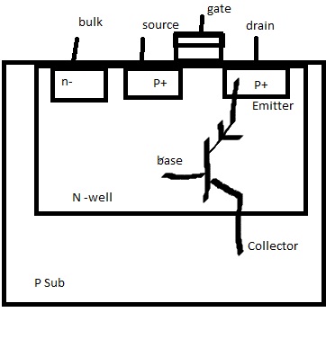
") ). From the fig. we can see that the collector and the substrate are the same, so can be just short the two terminals?
). From the fig. we can see that the collector and the substrate are the same, so can be just short the two terminals?