Continue to Site

Welcome to EDAboard.com

Welcome to our site! EDAboard.com is an international Electronics Discussion Forum focused on EDA software, circuits, schematics, books, theory, papers, asic, pld, 8051, DSP, Network, RF, Analog Design, PCB, Service Manuals... and a whole lot more! To participate you need to register. Registration is free. Click here to register now.

base current divider in npn common emiiter amplifier

Status
Not open for further replies.

yefj

Advanced Member level 4
Joined
Sep 12, 2019
Messages
1,174
Helped
1
Reputation
2
Reaction score
3
Trophy points
38
Activity points
7,056
Hello, i am using the data sheet shown bellow.
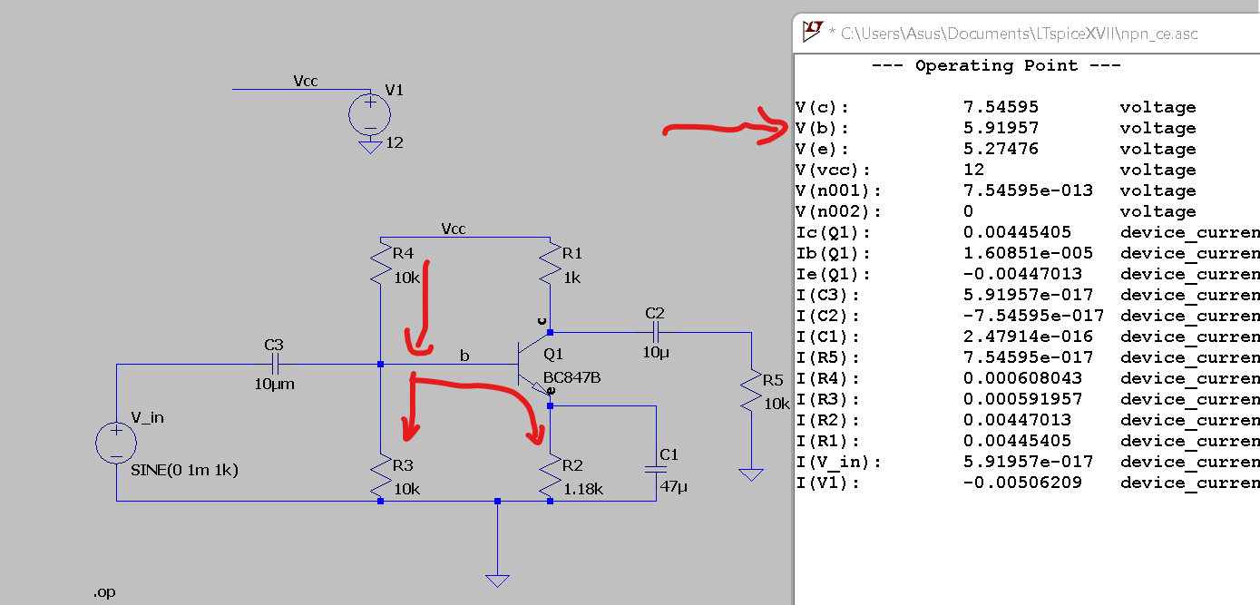
my Vcc is 12V i have put a 10k 10k ressistor ash shown bellow.
but instead of getting Vb=6 i get 5.91.
Is there some mathematical logic which could help me see how the current divides between R3 and base of bjt?
Thanks.
1678533892856.png
 

Hello,

basically, the emitter resistor R2 is approximatively seen multiplied by the h21 parameter of Q1 in parallel with R3
 

Hello, the root of the problem is predicting the correct value of Vbe for the transistor.
from the daa sheet i need Vce=5V and I_c=10mA
my Vce from simualtion is 2V as shown bellow.
How exactly do i play with the circuit in order to be sure i will be having Vbe of 0.7V as in the data sheet?

1678539836535.png


1678540241176.png
 

from the daa sheet i need Vce=5V and I_c=10mA
Need this values to achieve what? 10 mA can't be achieved with present R1 and R2 values, even in transistor saturation (amplifier not working). With given values for R1 and R2 (presume the values are well considered) you'll select an operation point that gives maximal undistorted output, e.g. Vce = 4V, Ic = 3.7 mA. Notice that Vce and Ic are linked and can't be chosen independently.

to be sure i will be having Vbe of 0.7V as in the data sheet
Vbe depends on Ic and temperature and also undergoes type variations. Notice the wide tolerance range in the datasheet line you have quoted above. Respectively it makes little sense to calculate Vbe with two decimal places.
You'll select R3 and R4 so that you come near to the optimal operation point for a typical transistor and an average transistor temperature.
 

Hello FVM, if i want Vce = 4V, Ic = 3.7 mA .
is there some mathematical expressions i can use to get these values?
Thanks.
 

Calcuate V(e), read typical Vbe for 4 mA from datasheet, e.g. 0.65 V, calculate V(b), calculate Rin = R2*B for typical gain value B. Select R3 and R4 for V(b) value considering Rin in parallel to R3, e.g. choose R3, calculate R3|| Rin, calculate optimal R4.
 

Hi,

(again you use a crappy datasheet form second source.Why not a detaile datasheet directly from the manufacturer?)

I´d say an accurate V_BE is not very important. (it drifts with temperature anyways)
Also h_FE varies in a wide range. So you can´t get a very accurate estimation.

You say you want V_CE = 4V. This leaves 8 V for R1 + R2.
also you say you want I_C to 3.7mA, this makes a voltage drop of 3.7V across R1. (Ohm´s law)
so 12V supply, 3.7V on R1, 4V on the bjt, leaves 4.3V for R2.
4.3V on 1.18 k makes 3.6mA.

I_E = I_C + I_B ... thus - according your requirements - means -0.1mA at the base. This is impossible.
--> you need to adjust your requirements.

Klaus
 

Hello, the root of the problem is predicting the correct value of Vbe for the transistor.
from the daa sheet i need Vce=5V and I_c=10mA
No, that is not the correct understanding of the main problem.
You cannot - and it is not necessary to - "predict the correct value of Vbe".
The BJT is a voltage-controlled device and the corresponding expression Ic=f(Vbe/Vt) follows an e-function.
This function is relatively steep with a factor Io which is very temperature-sensitive and has large tolerances. Therefore, you cannot find the "correct Vbe".

Therefeore, it is common practice to use negative DC feedback (mostly in form of an emitter resistor Re).
It is one of the consequences of negative feedback to make the properties of whole circuit less sensitive to active parameters.
As a consequence., it is sufficient to use a standard value for Vbe (0.65...0.75 volts).
As a result, the required base voltage Vb is found using the relation Vb=Ve+Vbe with Ve=Ie*Re.

In addition, it is recommended to use a relatively low-resistive base voltage divider for providing a voltage Vb as "stiff" as possible, that means: Less resistive to large tolerances of the base current Ib.
 
Last edited:

A good design is only followed by good design specs. If the design needs improvement start with better specs 1st.

e.g. DC bias of all nodes, input & output impedance , and frequency breakpoints. maximum C size, power consumption, etc

Here you go. https://tinyurl.com/2eerem43 online simulations
 
Status
Not open for further replies.

Similar threads

Part and Inventory Search

Welcome to EDABoard.com

Sponsor

Back
Top